Method for making spectrally efficient photodiode structures for CMOS color imagers

a color imager and photodiode technology, applied in the direction of electrical equipment, semiconductor devices, radio frequency controlled devices, etc., can solve the problems of poor color fidelity, poor color fidelity, and not economically practicabl

Inactive Publication Date: 2003-02-11
TAIWAN SEMICON MFG CO LTD
View PDF13 Cites 58 Cited by
  • Summary
  • Abstract
  • Description
  • Claims
  • Application Information

AI Technical Summary

Problems solved by technology

Although the CCD is a convenient device for photoimaging, it is not as economically practical as the CMOS image sensor for integrating other (camera) circuit functions on the same sensor chip for image processing.
This results in poor color fidelity of the original color image.
This poor color fidelity is a result of the nonuniform quantum efficiency (QE) across the optical waveband from 450 to 650 nm.

Method used


Image

  • Method for making spectrally efficient photodiode structures for CMOS color imagers
  • Method for making spectrally efficient photodiode structures for CMOS color imagers
  • Method for making spectrally efficient photodiode structures for CMOS color imagers

Examples


Embodiment Construction

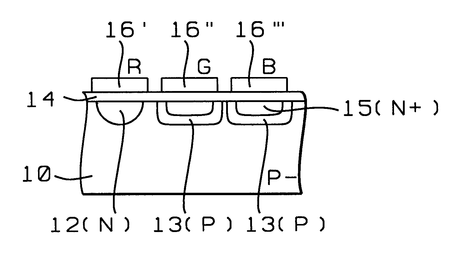
To better appreciate the invention for making these photodiodes with improved uniformity across the spectral range, the quantum efficiency (QE) of these photodiodes was determined as a function of optical wavelength. The QE was determined by simulating the collector efficiency as a function of optical wavelength for the N well photodiodes 12(N) and the N.sup.+ photodiodes 15(N.sup.+) formed in the P wells 13(P) for the photodiodes depicted in FIG. 4. The QE was simulated using a Medici simulation program provided by Avanti Corp. of U.S.A. FIG. 5 shows a plot of a curve 8 for the collector efficiency vs. the optical wavelength in micrometers for the deep N well red photodiode 12(N). As depicted in FIG. 5, the QE is about maximum (60%) at the long wavelength (650 um) for the red light, and the QE drops off dramatically to about 50% at the shorter wavelengths (450 um) for the blue light. FIG. 6 shows a plot of a curve 9 for the collector efficiency vs. the optical wavelength in microme...


PUM


Abstract

A method for making an array of photodiodes with more uniform optical spectral response for the red, green, and blue pixel cells on a CMOS color imager is achieved. After forming a field oxide on a substrate to electrically isolate device areas for CMOS circuits, an array of deep N doped wells is formed for photodiodes for the long wavelength red pixel cells. An array of P doped well regions is formed adjacent to and interlaced with the N doped wells. Shallow diffused N+ regions are formed within the P doped wells for the shorter wavelength green and blue color pixels cells. The shallow diffused photodiodes improve the quantum efficiency (QE), and provide a color imager with improved color fidelity. An insulating layer and appropriate dye materials are deposited and patterned over the photodiodes to provide the array of color pixel cells. The N and P doped wells are also used for the supporting FET CMOS circuits to provide a cost-effective manufacturing process.

Description

(1) Field of the InventionThe present invention relates to the fabrication of a CMOS color imager on a semiconductor substrate using CMOS technology, and more particularly relates to a method for making photodiodes with improved (more uniform) spectral response across the frequency band for the red, green, and blue (wavelength) pixel cells in the array of photodiodes.(2) Description of the Prior ArtIn camcorders and early digital cameras, charge coupled devices (CCDs) were used as optical detectors for detecting and processing color images. The CCDs detect the light on an array of photosites on the surface of an image sensor, and then the induced charge at each site in a row of the array of photosites is sequentially transferred to a readout register where it is detected, amplified, and processed through an analog / digital converter and stored as digital information for further processing. Although the CCD is a convenient device for photoimaging, it is not as economically practical a...

Claims


Application Information

Patent Timeline
Patent Type & Authority Patents(United States)
IPC IPC(8): H01L27/146
CPCH01L27/14645
Inventor WANG, CHING-CHUNYAUNG, DUN-NIANTSENG, CHIEN-HSIENWUU, SHOU-GWO
Owner TAIWAN SEMICON MFG CO LTD
Why Eureka
Try Eureka