Display device

a display device and display technology, applied in the direction of luminescnet screens, discharge tubes, identification means, etc., can solve the problems of increased current consumption, impaired reliability of el display devices, and inability to maintain accurate gray scale display

Inactive Publication Date: 2003-03-04
SEMICON ENERGY LAB CO LTD
View PDF6 Cites 226 Cited by
  • Summary
  • Abstract
  • Description
  • Claims
  • Application Information

AI Technical Summary

Problems solved by technology

Therefore the accuracy in gray scale display cannot be maintained, contributing to impaired reliability of EL display devices.
Furthermore, current consumption is increased when the amount of current flowing through the EL element is increased.
Moreover, bottom gate TFTs have the following two problems.
If a polycrystalline film such as a polysilicon film is used as the convex semiconductor thin film, the crystallinity of the film is inferior to that of a polycrystalline film formed on a flat surface, and characteristics such as an electric field effect mobility (mobility) are also poor.
Because of these problems, the frequency characteristic of a driver circuit composed of a bottom gate TFT is inferior to the frequency characteristic of a driver circuit composed of a top gate TFT.
Accordingly, the operation speed is insufficient especially in a source signal line driving circuit that uses a bottom gate TFT.

Method used


Image

  • Display device
  • Display device
  • Display device

Examples


embodiment 1

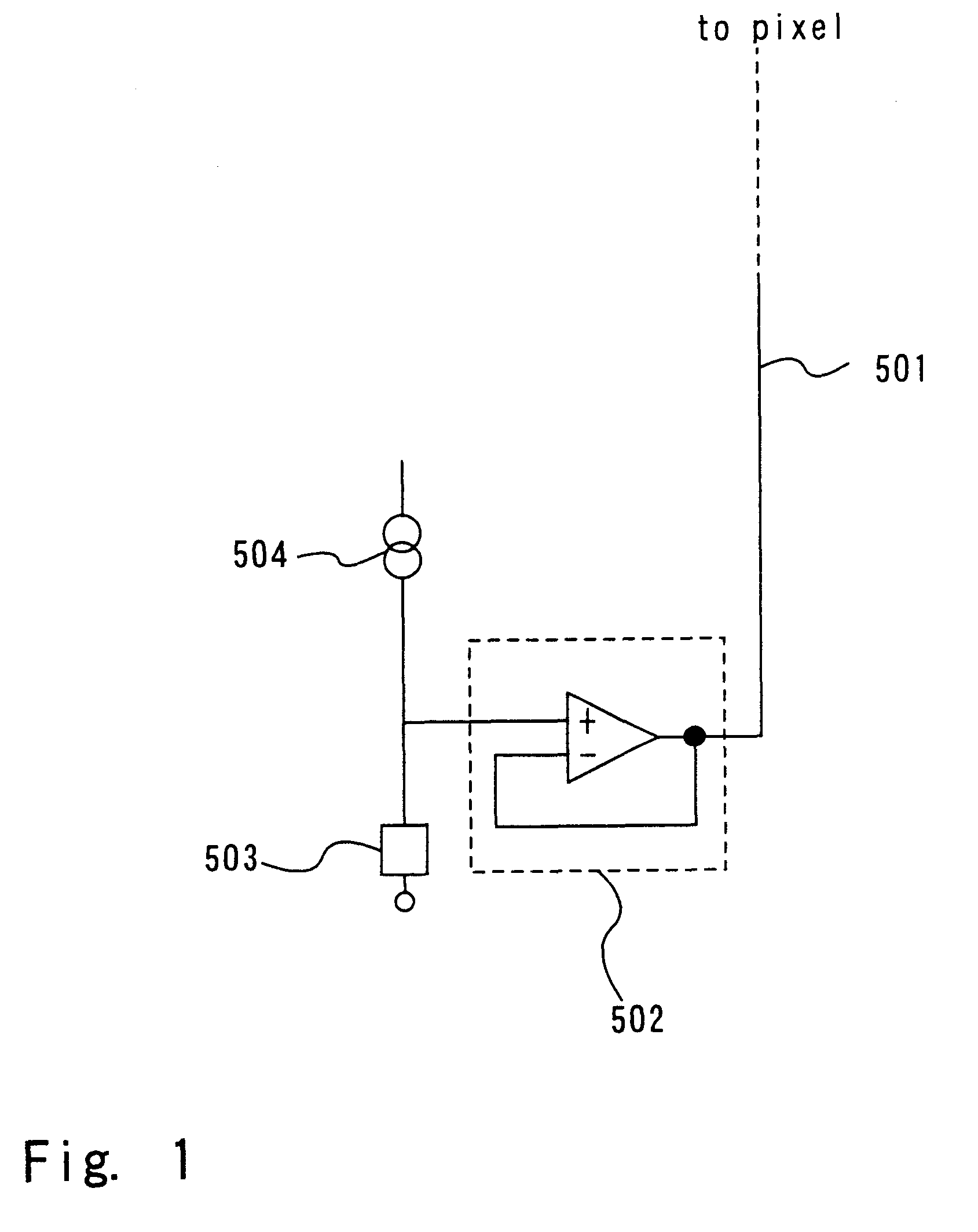
This embodiment gives a description about a case of using a temperature compensation circuit having a structure different from the structure shown in FIG. 1 in accordance with Embodiment Mode 1.

FIG. 2 shows the structure of a temperature compensation circuit according to this embodiment.

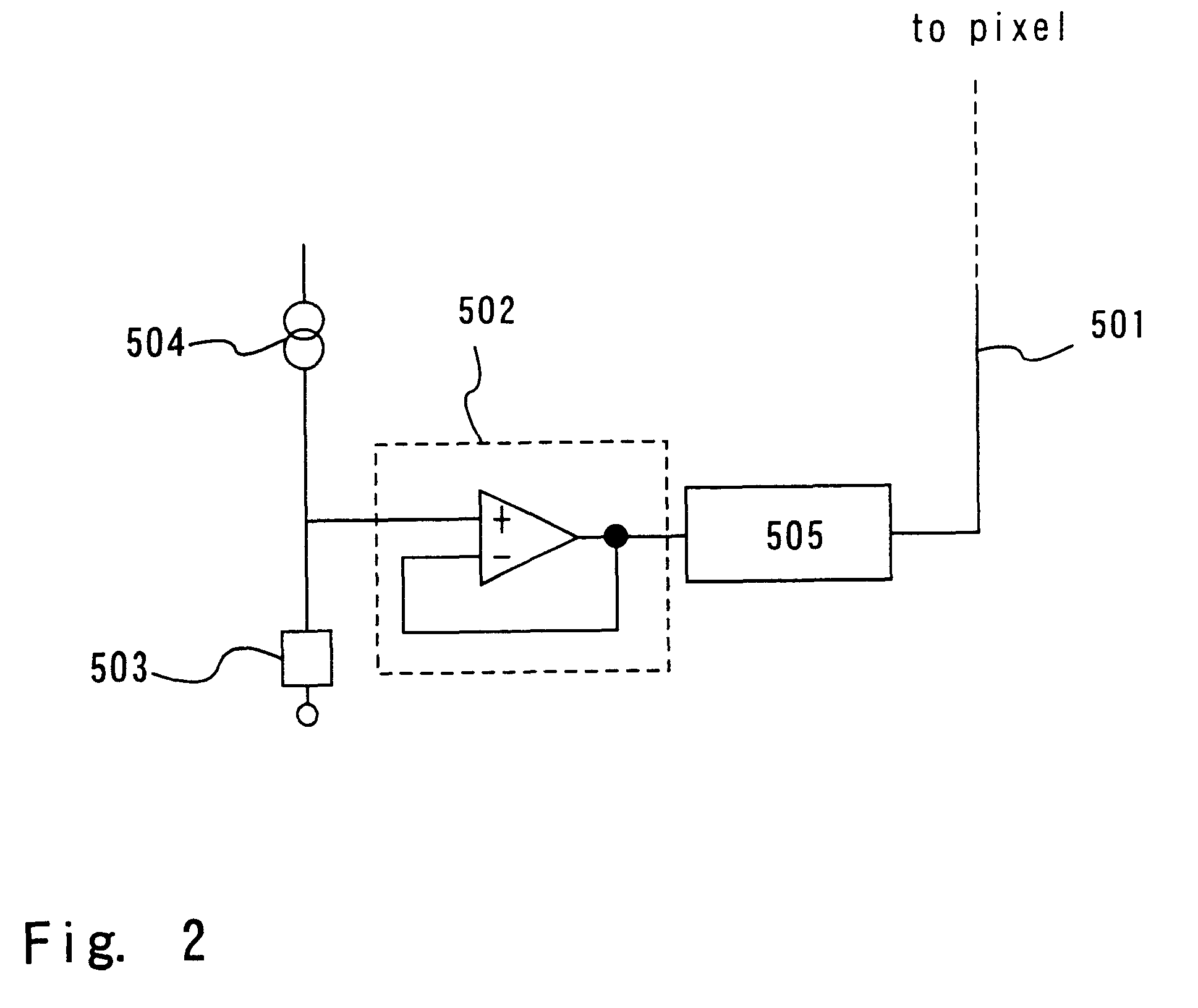
Reference symbol 501 denotes a power supply line, 502, a buffer amplifier, 503, a monitoring EL element, 504, a constant current generator, and 505, an adder circuit. One electrode of the monitoring EL element 503 is connected to the constant current generator 504, so that a constant amount of current flows through the monitoring EL element 503. When the temperature of an EL layer of the EL element changes, the amount of current flowing into the monitoring EL element 503 does not change but instead the electric potential of the electrode of the monitoring EL element 503 which is connected to the constant current generator 504 changes.

The monitoring EL element 503 and an EL element (not shown) in each...

embodiment 2

A description given in this embodiment is on an example of the structure of a buffer amplifier in a temperature compensation circuit of a display device according to the present invention.

FIG. 8 shows a case of manufacturing the buffer amplifier from a TFT that has the same structure as a TFT in a pixel.

The buffer amplifier is composed of TFTs 1901 to 1909, a capacitor 1910, constant current generators 1911 and 1912, and power supply lines 1930 and 1931.

The description given here takes as an example the case in which the TFTs 1901, 1902, 1906 and 1909 are n-channel TFTs whereas the TFTs 1903 to 1905 and the TFTs 1907 and 1908 are p-channel TFTs.

The electric potential of the power supply line 1930 at this point is set higher than the electric potential of the power supply line 1931. The electric potential of the power supply line 1931 is 0 V in FIG. 8, but it is not limited thereto.

The polarity of the TFTs according to this embodiment is not limited to the above. That is, any of the ...

embodiment 3

This embodiment describes a method of simultaneously manufacturing TFTs for a pixel portion of a display device according to the present invention and TFTs for driver circuit portions that are provided in the periphery of the pixel portion. To simplify the description, a CMOS circuit that is a basic unit of a driver circuit is illustrated as the driver circuit portions.

Referring to FIGS. 19A to 19E, gate electrodes 502 to 505 are first formed from a chromium film on a glass substrate 501. A silicon oxynitride film (an insulating film of SiOxNy) is used to form a gate insulating film 507 on the gate electrodes. On the gate insulating film 507, an amorphous silicon film is formed and crystallized by laser annealing. The crystallized film is patterned to form semiconductor films 508 to 511 that are crystalline silicon films. The steps up through this point can be carried out with known materials and known techniques. (FIG. 19A)

Next, insulating films 512 to 515 are formed from a silicon...


PUM


Abstract

The image quality of a display device using a bottom gate TFT is improved. In particular, fluctuation in luminance is controlled and the frequency characteristic of a driver circuit is compensated by suppressing a change in amount of current flowing through an EL element which is caused by a change in surrounding temperature while the device is in use. A monitoring EL element is provided in addition to a pixel portion EL element. The monitoring EL element constitutes a temperature compensation circuit together with a buffer amplifier and the like. A current is supplied to the pixel portion EL element through the temperature compensation circuit. This makes it possible to keep the amount of current flowing through the pixel portion EL element constant against a change in temperature, and to control the fluctuation in luminance. An input signal is subjected to time base expansion to perform sampling with accuracy.

Description

1. Field of the InventionThe present invention relates to an electronic display device fabricated by forming EL (electroluminescence) elements on a substrate, specifically, to an EL display device using a semiconductor element (an element formed from a semiconductor thin film). The invention also relates to electronic equipment employing the EL display device as a display unit.The EL element herein includes both an element that utilizes light emission from a singlet exciton (fluorescence) and an element that utilizes light emission from a triplet exciton (phosphorescence).2. Description of the Related ArtDevelopment of EL display devices having an EL element as a self-luminous element is flourishing in recent years. The EL display devices are also called organic EL displays (OELDs) or organic light emitting diodes (OLEDs).The EL display devices are self-luminous unlike liquid crystal display devices. The EL element is structured such that an EL layer is sandwiched between a pair of ...

Claims


Application Information

Patent Timeline
Patent Type & Authority Patents(United States)
IPC IPC(8): G09G3/38G09G3/10G09G3/30G09F9/30G09G3/04G09G3/32G09G3/34H01L31/12H01J1/00H01L27/15H01J1/62H05B33/00G09G3/20
CPCG09G3/2022G09G3/3233G09G2300/0842G09G2320/045G09G2320/029G09G2320/041G09G2320/043G09G2310/027
Inventor YAMAZAKI, SHUNPEIKOYAMA, JUNHOSOKI, KAZUE
Owner SEMICON ENERGY LAB CO LTD
Why Eureka
Try Eureka