Method of forming a film in a chamber and positioning a substitute in a chamber

a technology of silicon nitride and chamber, applied in the field of deposition technologies, can solve the problems of metal outgassing from the chamber, increased risk of failure of the formed integrated circuit device, and potential contamination of the susceptor

Inactive Publication Date: 2003-03-11
APPLIED MATERIALS INC
View PDF13 Cites 42 Cited by
  • Summary
  • Abstract
  • Description
  • Claims
  • Application Information

AI Technical Summary

Problems solved by technology

Such temperatures tend to cause outgassing of metals from the chamber into or on a semiconductor wafer.
Metal contamination of a semiconductor wafer is undesirable because i

Method used


Image

  • Method of forming a film in a chamber and positioning a substitute in a chamber
  • Method of forming a film in a chamber and positioning a substitute in a chamber
  • Method of forming a film in a chamber and positioning a substitute in a chamber

Examples


example 2 and example 3

show a precoat to the inside of a processing chamber according to the invention. Example 2 illustrates a situation where the chamber has not been pre-cleaned. Example 3 illustrates a situation where the chamber was subjected to a plasma clean prior to the pre-coat treatment. Contaminants from prior cleaning treatments have been known to contaminate wafers during processing steps. As reflected here, both examples 2 and 3 show a significant decrease in metal contamination in the film. In summary, Table I shows that precoating the processing chamber significantly decreases contamination in a film on a wafer even where the film formation follows a cleaning step.

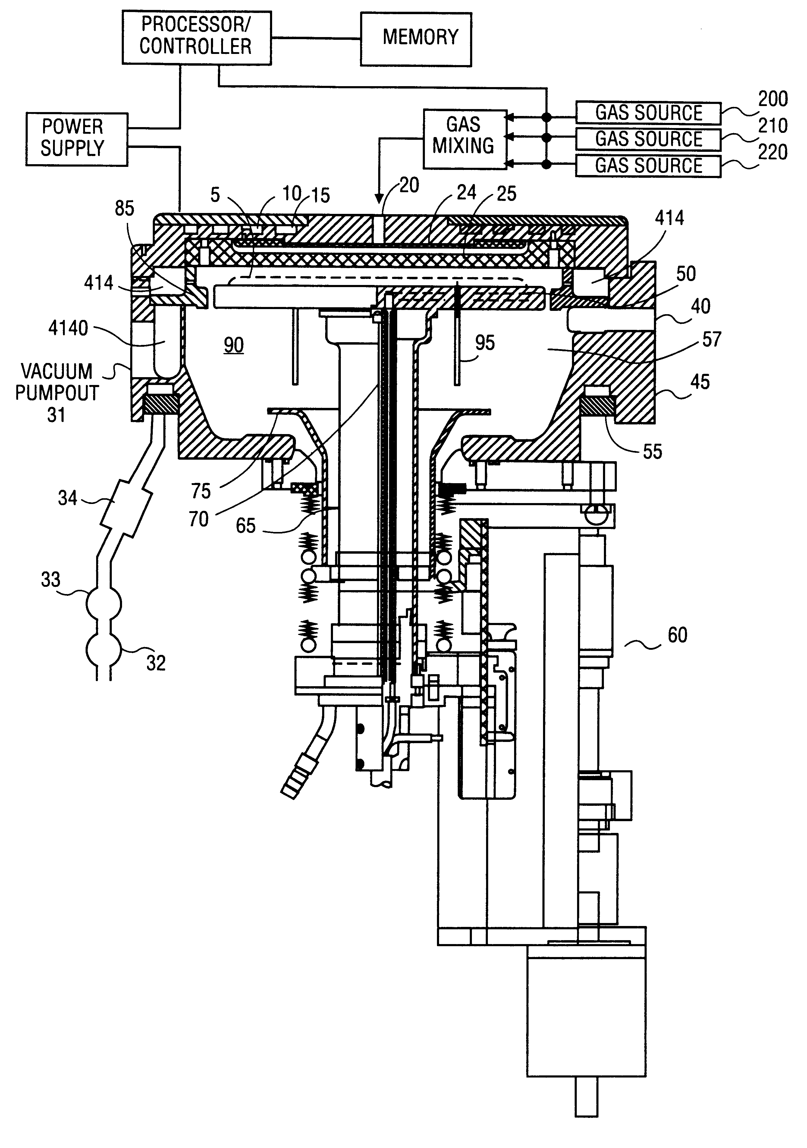
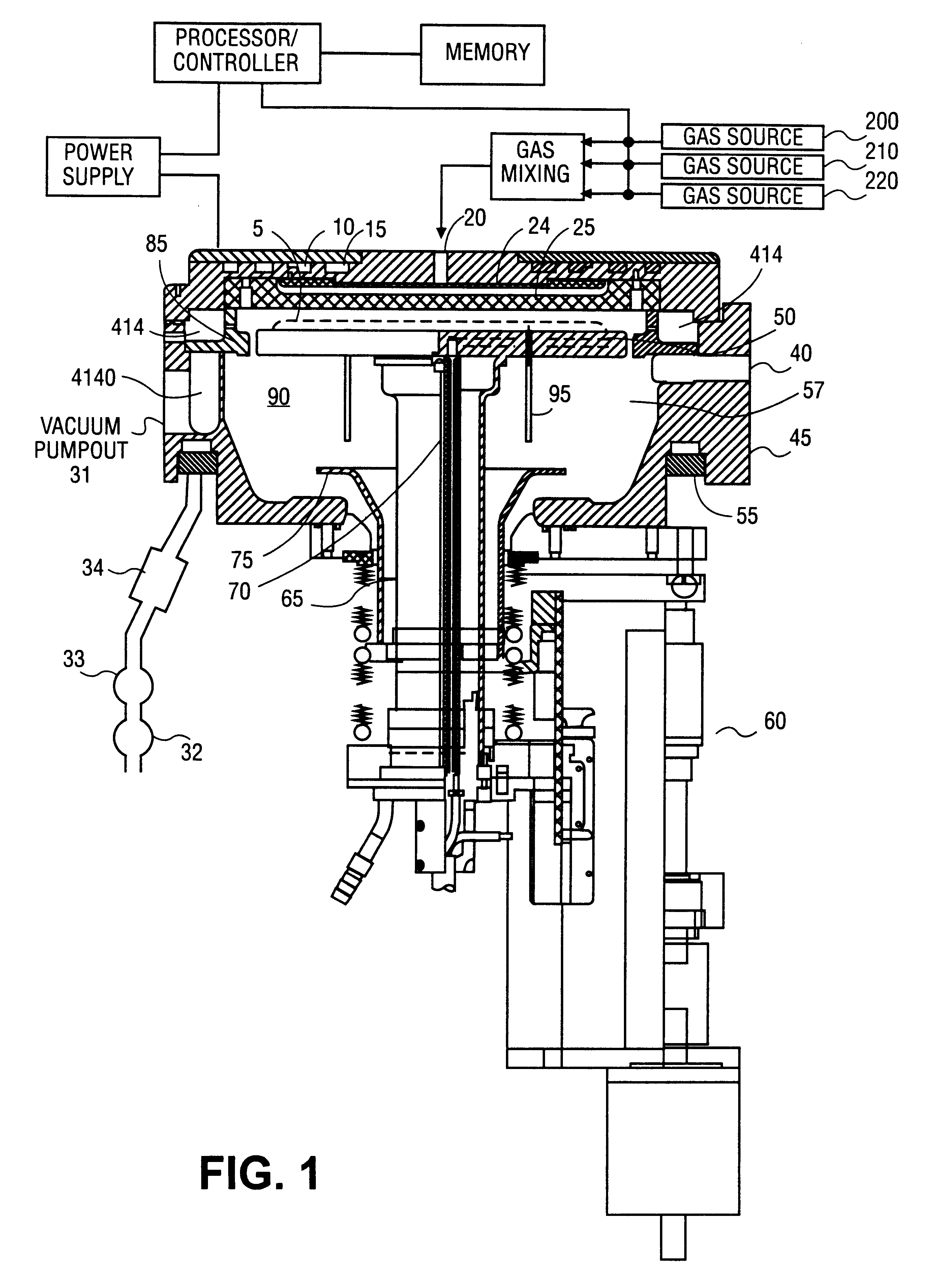
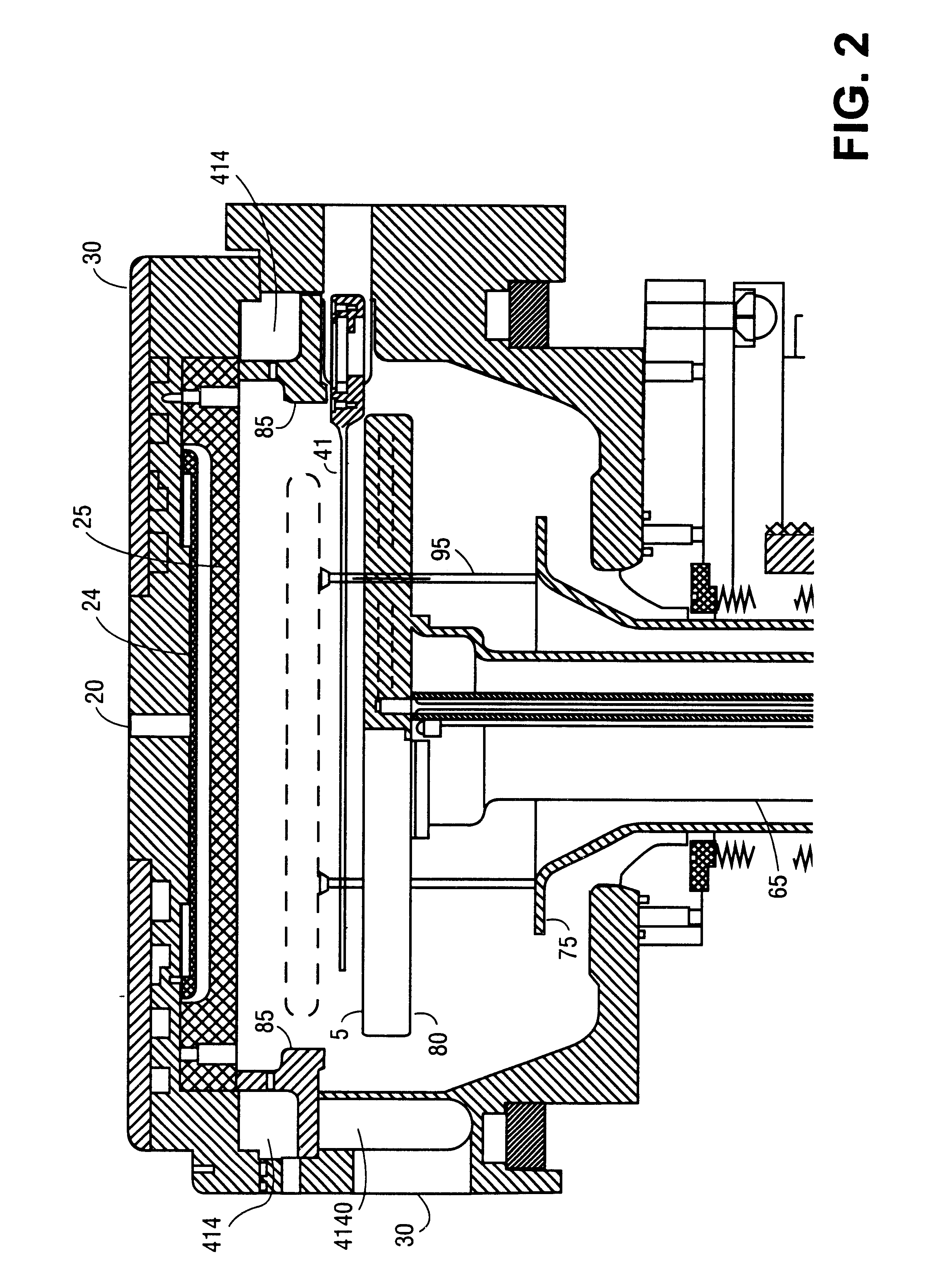
It is to be appreciated that the pre-treatment of a chamber to reduce contamination during processing is not limited to Si.sub.3 N.sub.4 film processing or use with resistively-heated processing chambers such as described above. Instead, the invention finds use in many other environments where wafer (or other substrate) contamina...


PUM

PropertyMeasurementUnit
Pressureaaaaaaaaaa
Pressureaaaaaaaaaa
Angleaaaaaaaaaa

Abstract

Methods and apparatuses of forming a film on a substrate including introducing a pretreatment material into a processing chamber sufficient to form a film as a portion of an inner surface of the processing chamber to inhibit outgassing from that portion of the chamber, introducing a substrate into the chamber, and forming a film on the substrate.

Description

1. Field of the InventionThis invention relates generally to deposition technologies in integrated circuit chip processing and more particularly to the deposition of silicon nitride films.2. Discussion of Related ArtThe manufacture of integrated circuits generally involves the formation of a plurality of layers of material on a semiconductor (e.g., silicon) wafer in a processing chamber, each layer serving a specific function generally related to the routing and isolation of specific signals. Temperatures in a processing chamber during these formation processes may reach 800.degree. C. to 850.degree. C. Such temperatures tend to cause outgassing of metals from the chamber into or on a semiconductor wafer. Metal contamination of a semiconductor wafer is undesirable because it increases the risk of failure of the integrated circuit devices formed from the wafer.It is desirable to provide a method that reduces or prevents outgassing of metals from the chamber to a semiconductor wafer.M...

Claims


Application Information

Patent Timeline
IPC IPC(8): H01L21/00
CPCH01L21/67017
Inventor YANG, MICHAEL X.HO, HENRYCHEN, STEVEN A.
Owner APPLIED MATERIALS INC
Why Eureka
Try Eureka