Multilayer wiring board and semiconductor device

a wiring board and semiconductor technology, applied in the field of multi-layer wiring boards, can solve the problems of increasing the impedance, becoming difficult for the chip condenser to achieve the above object, and becoming impossible to reduce the film thickness of the interlayer insulating layer

Inactive Publication Date: 2003-04-08
SHINKO ELECTRIC IND CO LTD
View PDF7 Cites 60 Cited by
  • Summary
  • Abstract
  • Description
  • Claims
  • Application Information

AI Technical Summary

Benefits of technology

According to the above structure, the side wall of the second contact hole and the surface of the metallic base material exposed to the bottom of the first contact hole are separate from each other by the peripheral edge section of the first contact hole. Therefore, even when foreign objects such as particles enter the first and the second contact holes, it is difficult for the metallic layer for a condenser and the metallic base material to be short-circuited with each other. Therefore, the reliability of insulation between the metallic layer for a condenser electrode and the metallic base material can be enhanced.

Problems solved by technology

The reason is that when the length of the wiring between the chip condenser and the wiring layer is long, the impedance is increased, so that it becomes difficult for the chip condenser to accomplish the above object.
Therefore, it becomes impossible to reduce the film thickness of the interlayer insulating layer.
Further, when the film thickness is large, the cost of the interlayer insulating layer 204 is raised.
Therefore, the manufacturing cost of the multilayer wiring board 201 is increased.
Therefore, even when foreign objects such as particles enter the first and the second contact holes, it is difficult for the metallic layer for a condenser and the metallic base material to be short-circuited with each other.

Method used


Image

  • Multilayer wiring board and semiconductor device
  • Multilayer wiring board and semiconductor device
  • Multilayer wiring board and semiconductor device

Examples


Embodiment Construction

(1) Explanation of Multilayer Wiring Board of an Embodiment of the Present Invention

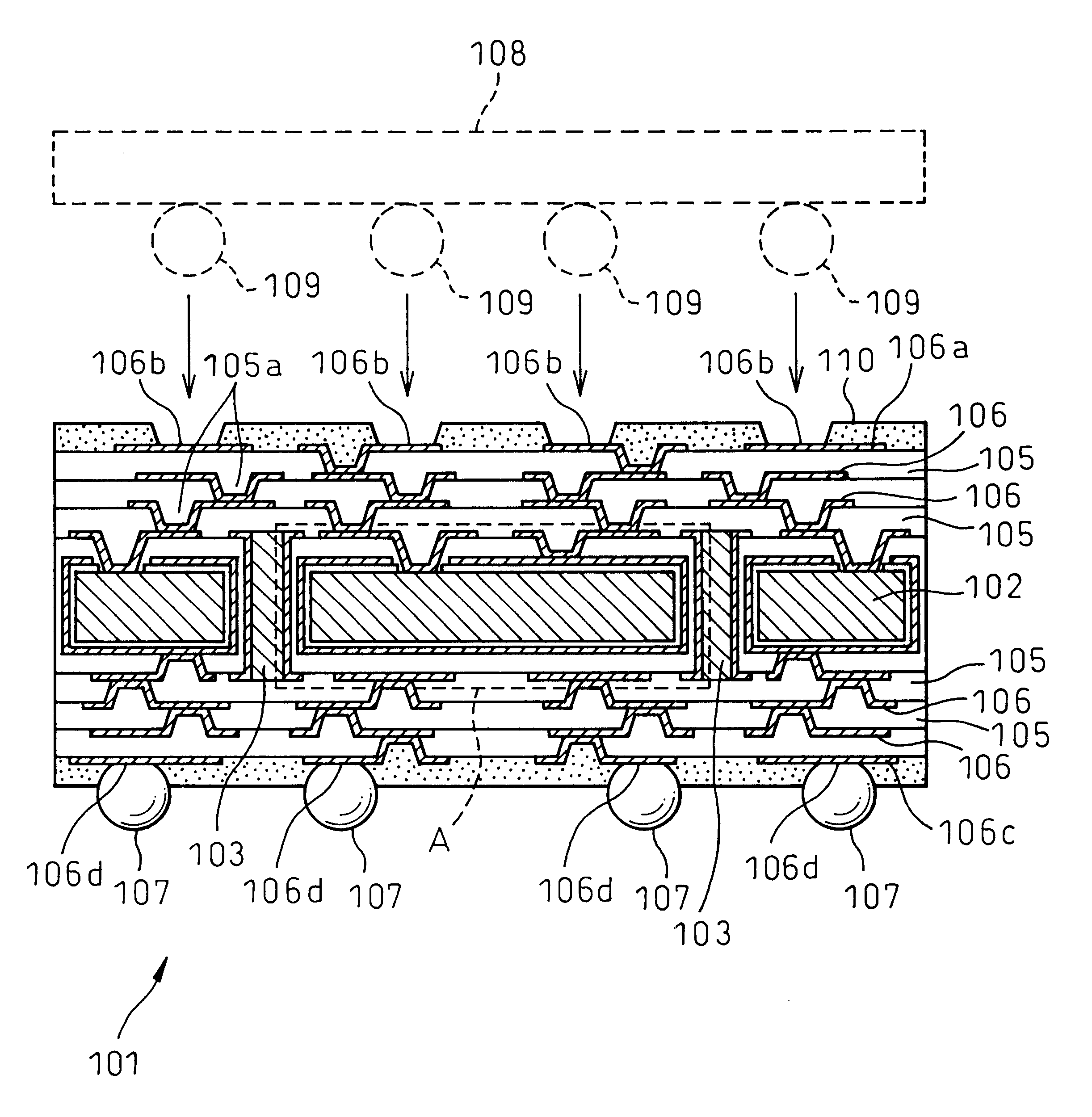
Next, a multilayer wiring board of an embodiment of the present invention will be explained referring to FIG. 1. FIG. 1 is a cross-sectional view showing a multilayer wiring board of an embodiment of the present invention.

The multilayer wiring board 101 of the embodiment of the present invention is composed in such a manner that a plurality of interlayer insulating layers 105, 105, . . . and a plurality of wiring layers 106, 106, . . . are alternately laminated on each other in an upper and a lower portion of the aluminum base material (metallic base material) 102. In this structure, the aluminum base material (metallic base material) 102 has a function of a core for increasing the mechanical strength of the entire multilayer wiring board 101. This function is the same as the function of the core base material (metal substrate) 202 of the conventional multilayer wiring board 201 shown in FIG. 6. Due ...


PUM


Abstract

A multilayer wiring board comprises: a metal substrate as a core, a condenser dielectric layer formed to cover the metal layer, and a condenser electrode metal layer formed to cover the condenser dielectric layer, so that a condenser is defined by the metal substrate, the condenser dielectric layer and the condenser electrode metal layer. Integral with the structure of the wiring board is a discrete capacitor component with the metal substrate and the condenser electrode forming the two plates thereof with the dielectric layer there between. The condenser dielectric layer is provided with a first contact hole to communicate with the metal substrate and the condenser electrode metal layer is provided with a second contact hole to communicate with the first contact hole, the diameter of the second contact hole being larger than that of the first contact hole. An insulating layer is formed on the condenser electrode metal layer and is provided with a via hole to communicate with the metal substrate through the second and first contact holes. A metal substrate contact metal layer formed on an inner wall of the via hole, so that the metal substrate contact metal layer comes into electrical contact with the metal substrate.

Description

1. Field of the InventionThe present invention relates to a multilayer wiring board. More particularly, the present invention relates to a multilayer wiring board inside which a condenser structure is composed and also relates to a method of manufacturing the multilayer wiring board. Further, the present invention relates to a semiconductor device into which the multilayer wiring board is incorporated and also relates to a method of manufacturing the semiconductor device.2. Description of the Related ArtRecently, the density of electronic equipment has been highly increased. Accordingly, a multilayer wiring board in which a plurality of wiring layers are laminated together has been realized. A multilayer wiring board of the prior art is shown in FIG. 6.The multilayer wiring board 201 of the prior art, shown in FIG. 6, includes a core base material 202 made of insulating material such as glass-epoxy resin or ceramics. On both sides of the core base material 202, there are provided a ...

Claims


Application Information

Patent Timeline
Patent Type & Authority Patents(United States)
IPC IPC(8): H01L23/58H01L23/64H01L23/498H01L23/48H05K3/44H05K1/16H05K3/46H05K1/14H05K1/05
CPCH01L23/49822H05K1/162H05K3/445H01L23/642H01L2924/01019H01L2224/16H01L2924/01078H01L2924/09701H01L2924/15311H01L2924/3011H05K1/053H05K1/056H05K1/141H05K3/4608H05K2201/0175H05K2201/0179H05K2201/09509H05K2201/09554H05K2201/09809H05K2203/0315
Inventor MASHINO, NAOHIRO
Owner SHINKO ELECTRIC IND CO LTD
Why Eureka
Try Eureka