Timing optimization in presence of interconnect delays

a timing optimization and delay technology, applied in the field of digital logic design systems, can solve the problems of inconvenient timing optimization, inconvenient timing optimization, and inability to accurately formulate the interconnect delay and optimal buffering scheme to minimize i

Inactive Publication Date: 2003-04-22
MAGMA DESIGN AUTOMATION
View PDF4 Cites 73 Cited by
  • Summary
  • Abstract
  • Description
  • Claims
  • Application Information

AI Technical Summary

Problems solved by technology

In many cases, the IC designer improperly connected or improperly placed a physical item within one or more cells.
Interconnect delay is a major concern in deep sub-micron technologies for two reasons: as the technologies scale, the feature sizes are shrinking.
The exact formulation of the interconnect delay and an optimal buffering scheme to minimize it can be very complex.
Since many of these parameters are dependent on specific net instances, a complex analysis / buffering strategy would have limited practical use when buffering a design with tens of thousands of long wires.
If no combination of wire delays can satisfy the timing constraints, the circuit cannot meet timing for the given selection of gate sizes.

Method used


Image

  • Timing optimization in presence of interconnect delays
  • Timing optimization in presence of interconnect delays
  • Timing optimization in presence of interconnect delays

Examples


Embodiment Construction

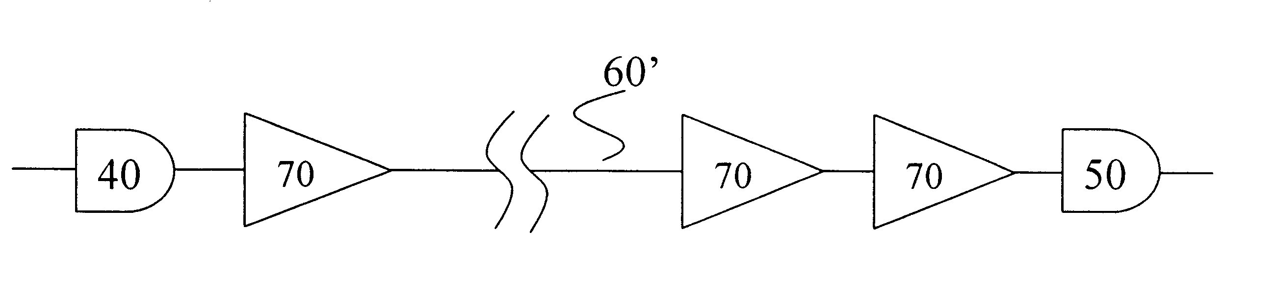
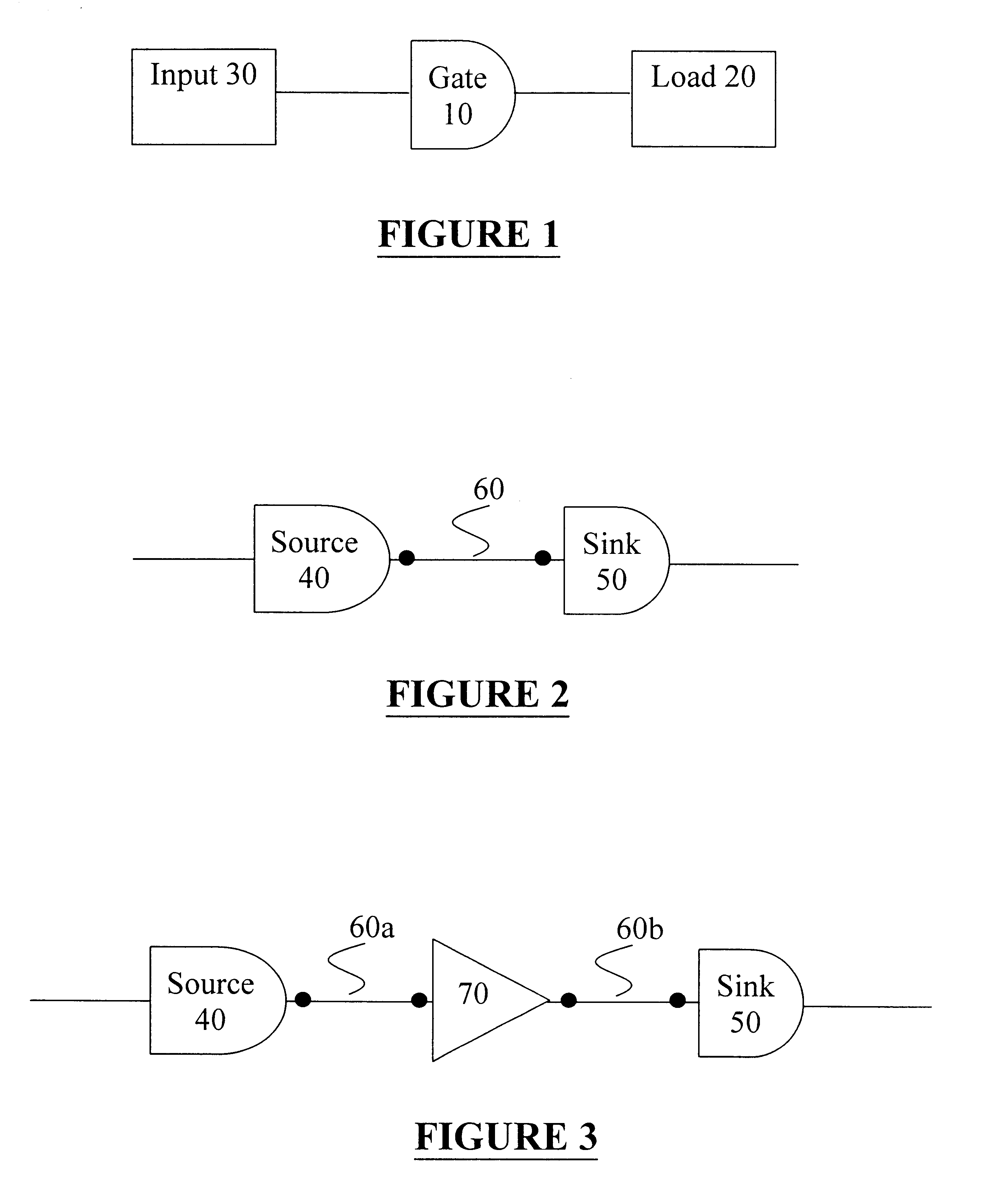
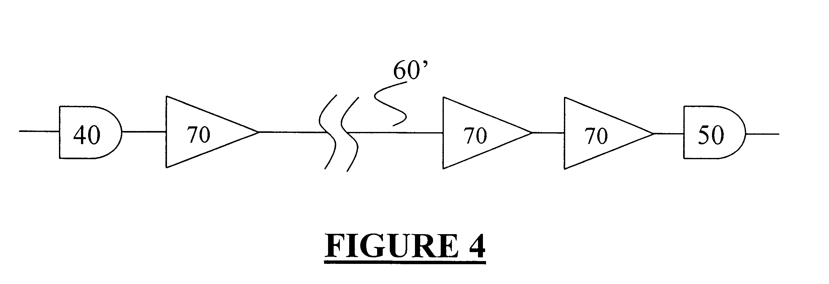
As is known in the art, the theory of logical effort represents the delay D.sub.gate through a simple logic gate 10 as shown in FIG. 1, driving a capacitive load 20 as:

D.sub.gate =.tau.(g.sub.gate h.sub.gate +p.sub.gate) (1)

where g.sub.gate is the logical effort of the gate, h.sub.gate is the electrical effort and p.sub.gate is the intrinsic delay of the gate. .tau. is a technology constant defined as the delay of an ideal inverter with no intrinsic delay, driving another ideal inverter.

The logical effort g.sub.gate represents the computational complexity of the gate and measures how much weaker it is in current drive compared to an ideal inverter with the same input capacitance. It compares the characteristic time constant (product of the output resistance and input capacitance) of a gate with that of an inverter. Logical effort is a function of the topology of the transistor interconnections but not of transistor sizes, and is given by: ##EQU1##

where gate_min refers to the minimum...


PUM


Abstract

A strategy for optimal buffering in the case of an infinitely long wire buffered with an arbitrary number of equally spaced single-size buffers is presented. A simple but efficient technique is proposed using this to choose a buffer size and determine a good inter-buffering distance up front, thus enabling fast, efficient buffer insertion. The analysis also allows representing delays of long wires as a simple function of the length and buffer and wire widths. Based on this, a novel constant wire delay approach is proposed where the proposed wire delay model is used for fairly accurate prediction of wire delays early in the design process and these predictions are later met via buffer insertion and wire sizing.

Description

1. Field of the InventionThe present invention is directed to digital logic design systems. More particularly, the invention is directed. to automated digital logic synthesis and placement systems.2. Background of the Related ArtPrior art computer aided design (CAD) systems for the design of integrated circuits and the like assist in the design thereof by providing a user with a set of software tools running on a digital computer. In the prior art, the process of designing an integrated circuit on a typical CAD system was done in several discrete steps using different software tools.First, a schematic diagram of the integrated circuit is entered interactively to produce a digital representation of the integrated circuit elements and their interconnections. This representation may initially be in a hardware description language such as Verilog and then translated into a register transfer level (RTL) description in terms of pre-designed functional blocks, such as memories and register...

Claims


Application Information

Patent Timeline
Patent Type & Authority Patents(United States)
IPC IPC(8): G06F17/50
CPCG06F17/505G06F17/5022G06F30/327G06F30/33G06F30/3312G06F2119/12G06F30/3308
Inventor BUCH, PREMAL V.SAVOJ, HAMIDVAN GINNEKEN, LUKAS P. P. P.
Owner MAGMA DESIGN AUTOMATION
Why Eureka
Try Eureka