

Dielectric resonator, dielectric filter, dielectric duplexer, and communication device
a technology of dielectric filters and dielectric duplexers, which is applied in the direction of resonators, electrical equipment, waveguides, etc., can solve the problems of dominant loss of conductors and the inability of techniques to meet the requirement of reducing the size of resonators
- Summary
- Abstract
- Description
- Claims
- Application Information
AI Technical Summary
Benefits of technology
Problems solved by technology
Method used
Image

Examples
first embodiment
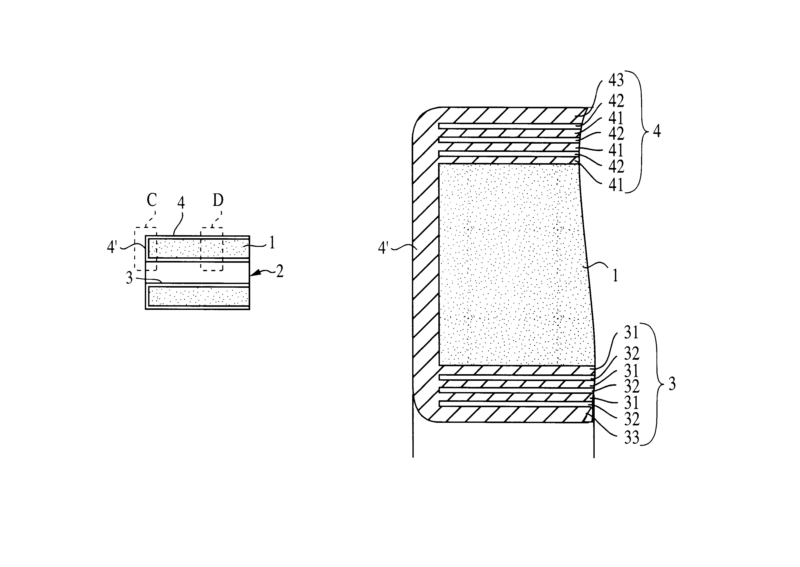
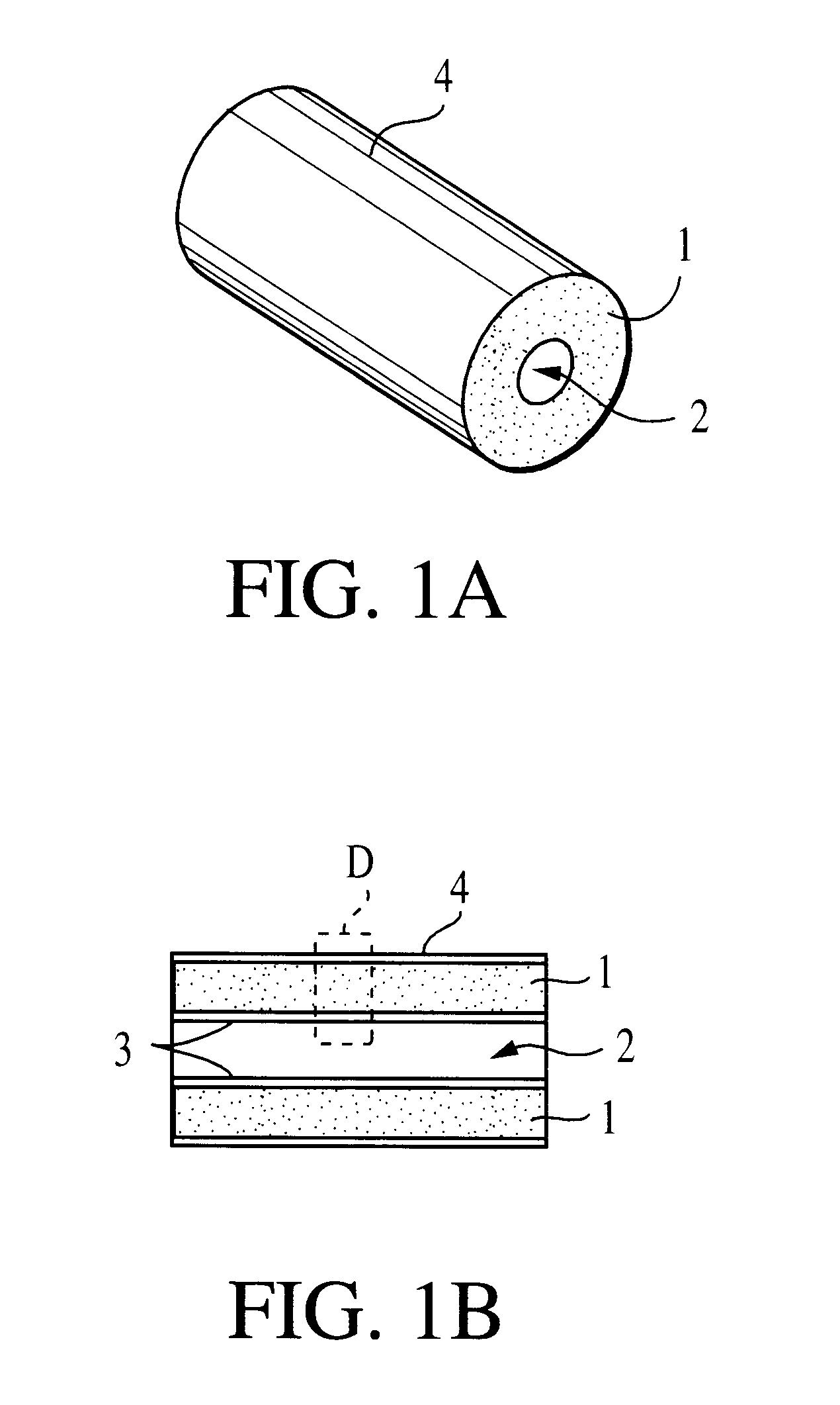
The structure of a dielectric resonator is described below with reference to FIGS. 1A, 1B and 2.
FIG. 1A is a perspective view illustrating the appearance of the dielectric resonator, and FIG. 1B is a cross-sectional view thereof taken along the central axis. In these figures, reference numeral 1 denotes a cylindrical-shaped dielectric block having a through-hole 2 extending along the central axis from one end face to the opposite end face. An inner conductor 3 is formed on the inner surface of the through-hole 2, and an outer conductor 4 is formed on the outer surface of the dielectric block 1. As will be described later, the inner conductor 3 and the outer conductor 4 are both formed so as to have a thin-film multilayer electrode structure consisting of a plurality of thin-film conductive layers and thin-film dielectric layers which are alternately disposed one on another.
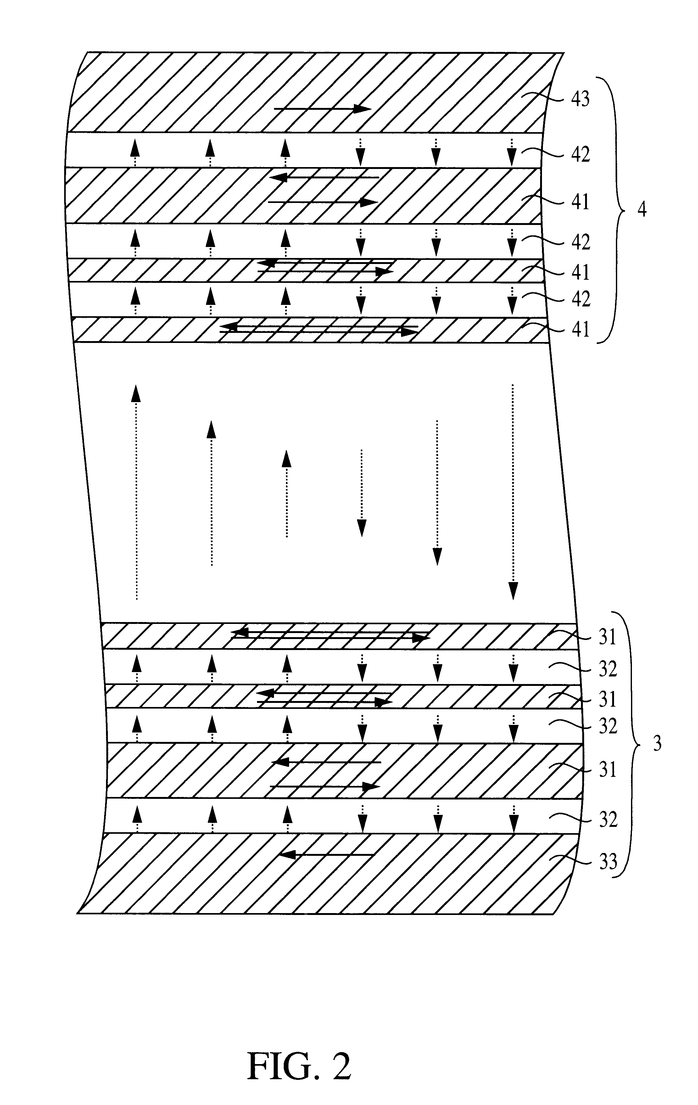
FIG. 2 is a cross-sectional view of a part denoted by D in FIG. 1B. Note that in FIG. 2 the thickness of the d...
second embodiment
The structure of a dielectric resonator is described below with reference to FIGS. 3A-3C.
FIG. 3A is a perspective view illustrating the appearance of the dielectric resonator, and FIG. 3B is a cross-sectional view thereof taken along the central axis. FIG. 3C is an enlarged view of a part denoted by C in FIG. 3B. In this embodiment, unlike the first embodiment described above with reference to FIGS. 1A-1B, one end face, on a front side in FIG. 3A, of a dielectric block 1 is formed so as to act as an open-circuited end, and the opposite end face is formed so as to act as a short-circuited end. An inner conductor 3 and an outer conductor 4 are formed on the inner surface of a through-hole 2 and the outer surface of the dielectric block 1, respectively, in a similar manner to the first embodiment. A part denoted by D in FIG. 3B has an electrode structure similar to that shown in FIG. 2, although the distributions of currents and displacement currents are different. An outer conductor ...
third embodiment
The structure of a dielectric filter is described below with reference to FIGS. 4, 5A and 5B.
FIG. 4 is a perspective view illustrating the appearance of the dielectric filter. Note that the dielectric filter is drawn such that the plane to be in contact with a mounting substrate is on the top side of FIG. 4. In FIG. 4, reference numeral 1 denotes a rectangular dielectric block. In the dielectric block 1, through-holes 2a and 2b are formed between two opposite end faces such that the axes thereof become parallel to each other. The through-holes 2a and 2b have a stepped structure in terms of the hole diameter along the axis thereof. That is, the through-hole 2a and 2b includes a small-diameter part with a small hole diameter formed in the center and large-diameter parts with a large hole diameter formed on both end sides. Inner conductors 3a and 3b are formed on the inner surfaces of the respective through-holes 2a and 2b. On the outer surface of the dielectric block 1, an outer cond...
PUM
 Abstract
Description
Claims
Application Information