

Use of static noise analysis for integrated circuits fabricated in a silicon-on-insulator process technology
a technology of silicon-on-insulator and process technology, applied in logic circuit coupling/interface arrangement, pulse technique, instruments, etc., can solve problems such as failure of circuits, inability to take into account significant methods, and insufficient methods which vary the behavior of all transistors in the network at the same tim
- Summary
- Abstract
- Description
- Claims
- Application Information
AI Technical Summary
Benefits of technology
Problems solved by technology
Method used
Image

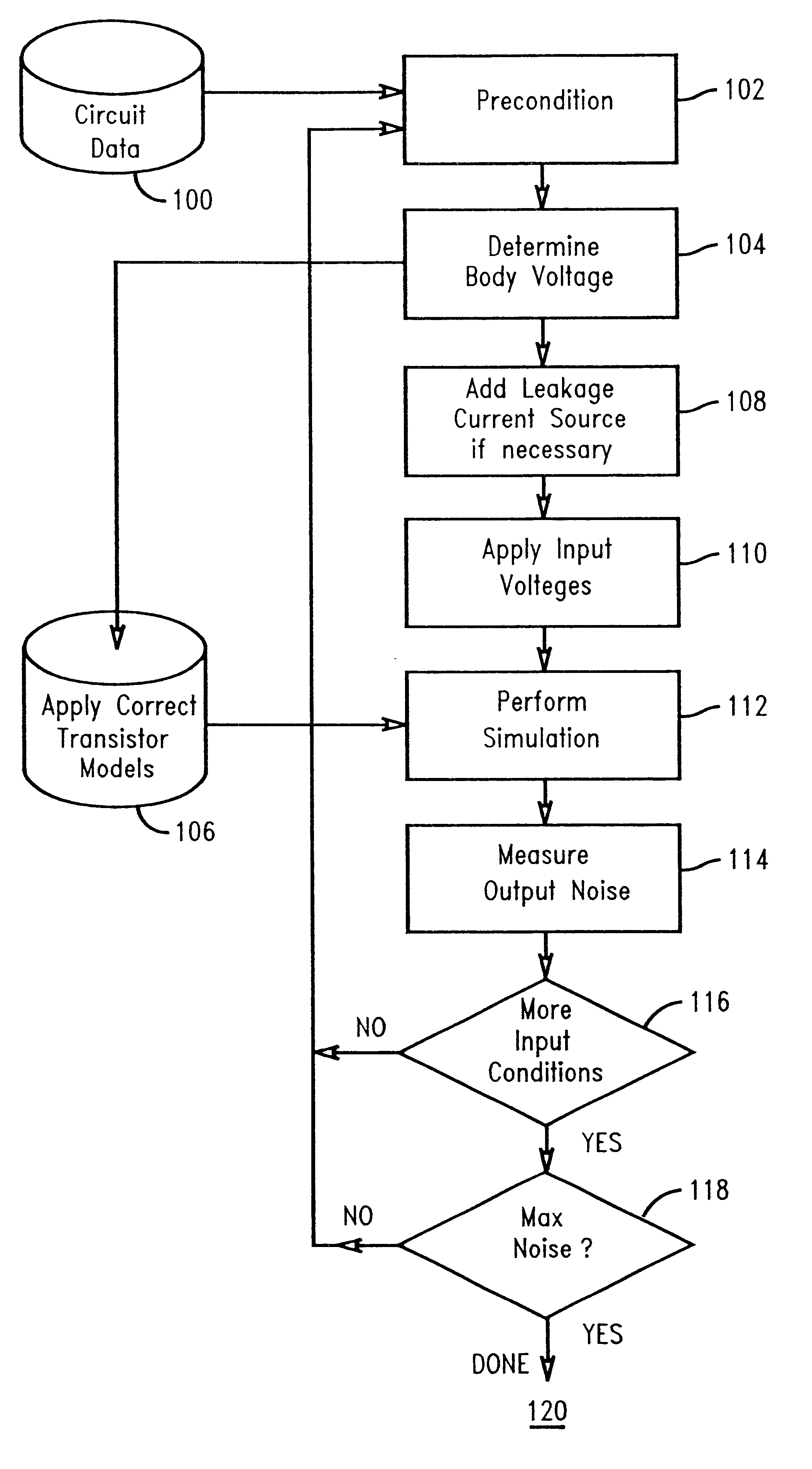
Examples
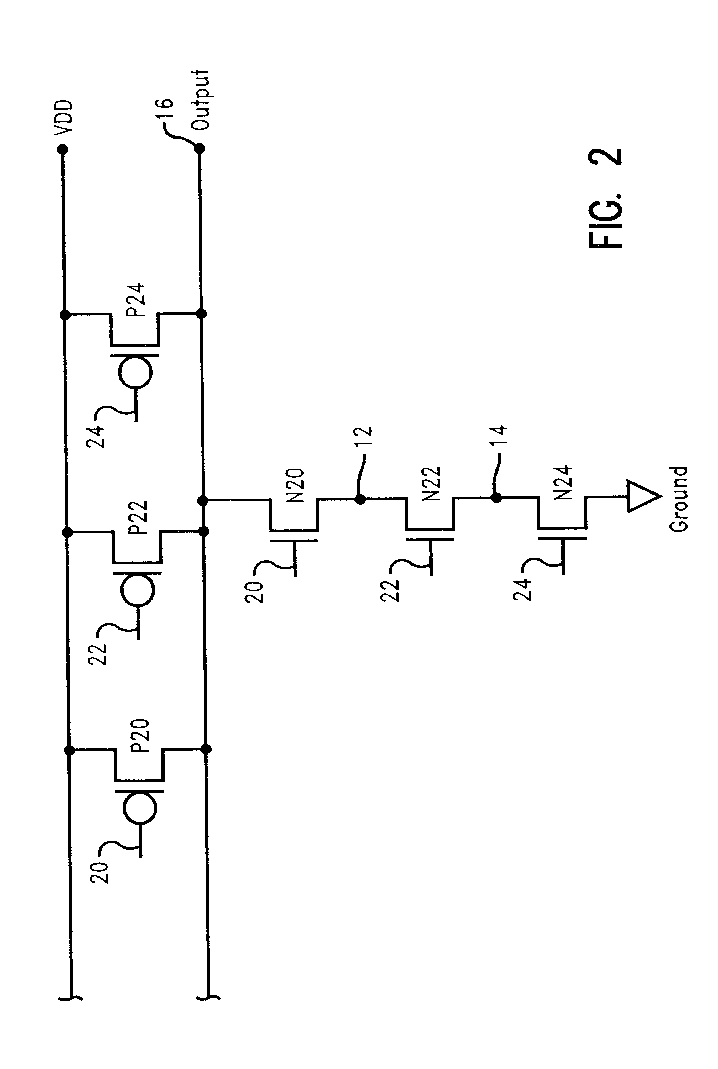
example 1 (fig.2)
Example 1 (FIG. 2)
FIG. 2 illustrates an injected noise analysis of a 3-way NAND circuit, accounting for hysteresis and bipolar leakage using the HOT / WARM / COLD modeling assignment and the addition of a leakage current source described in the preferred embodiment.
We describe the execution of the invention on the network of FIG. 2, where
P is used to represent a pFET device, and
N is used to represent a nFET device.
Input pins are labeled as 20, 22 and 24, and the output pin is labeled 16. The internal nodes are labeled as 12 or 14.
Step 1.
This circuit is described in the data model as an interconnection of nets, sources, and devices.
Step 2.
Input voltages are determined such that they precondition the circuit for a worst-case response to noise.
For this circuit, we have two possible output states, 1 and 0.
If the output is to be simulated for its affect on a stable output value of 1, there are several input voltage conditions which could be the worst preconditioning for noise.
case 1
20=0
Input 22=1
Input 24=1
This means output 16 is held high with one transistor, P20, conducting to Vdd.
This also means N20 and N22 are conducting, discharging the internal nodes, 12 and 14, to 0 or ground potential.
If input 20, while set to a logic 0, receives noise such that input 20's voltage rises from ground, N20 will conduct, perhaps even slightly, creating a path to ground, which will cause output 16 to dip below Vdd. How much the output dips is dependent on how much high-going noise is present on input 20, and how much N20 conducts as a result of that noise on input 20.
Step 3.
Review the circuit, its input voltages and device types (pFET or nFET). Select a device initial body voltage for each device, determined by the set of input voltages and the particular device type, using the rules outlined above. (In this example, input 20=0, 22=1 and 24=1).
1. P20 is conducting, with noise that may cause it to conduct less during simulation of the noisy input conditions. It is assigned a ...
example 2 (fig.3)
Example 2 (FIG. 3)
In FIG. 3, a schematic of a two-input dynamic NOR gate is shown. In this example, step 3 of example 1 is replaced with step 4, and only a leakage noise analysis is conducted.
The execution of the invention on the following network is described, where
P is used to represent a pFET device, and
N is used to represent an nFET device.
Input pins are labeled as 32, 34, CLKB 30 and CLK 36. The output pin is labeled 38. The internal node is labeled as 40.
Step 1
This circuit is described in the data model as an interconnection of nets, sources, and devices.
Step 2
Input voltages are determined such that they precondition the circuit for a worst-case response to noise.
In this case, we are only measuring leakage noise.
For example, initially, nFETs N32 and N34 are set to be off (input 32 and 34=0), and output 38 is precharged high. CLKB 30 is logic high (1) and CLK 36 is logic low (0).
If input 32 or 34 is high (1) during an evaluate phase (when CLK 36 is high (1)), output 38 will dis...
PUM
 Abstract
Description
Claims
Application Information