Additives to CMP slurry to polish dielectric films

a technology of additives and dielectric films, applied in the direction of polishing compositions, aqueous dispersions, chemistry apparatus and processes, etc., can solve the problems of dielectric materials being removed at different times, capacitative coupling between layers can adversely affect the operation of semiconductor devices, and the demand for processing capabilities

Inactive Publication Date: 2003-05-27
APPLIED MATERIALS INC
View PDF60 Cites 100 Cited by
  • Summary
  • Abstract
  • Description
  • Claims
  • Application Information

AI Technical Summary

Problems solved by technology

However, as the fringes of circuit technology are pressed, the shrinking dimensions of interconnects in VLSI and ULSI technology has placed additional demands on the processing capabilities.
Increased capacitative coupling between layers can detrimentally affect the operation

Method used


Image

  • Additives to CMP slurry to polish dielectric films
  • Additives to CMP slurry to polish dielectric films
  • Additives to CMP slurry to polish dielectric films

Examples


Embodiment Construction

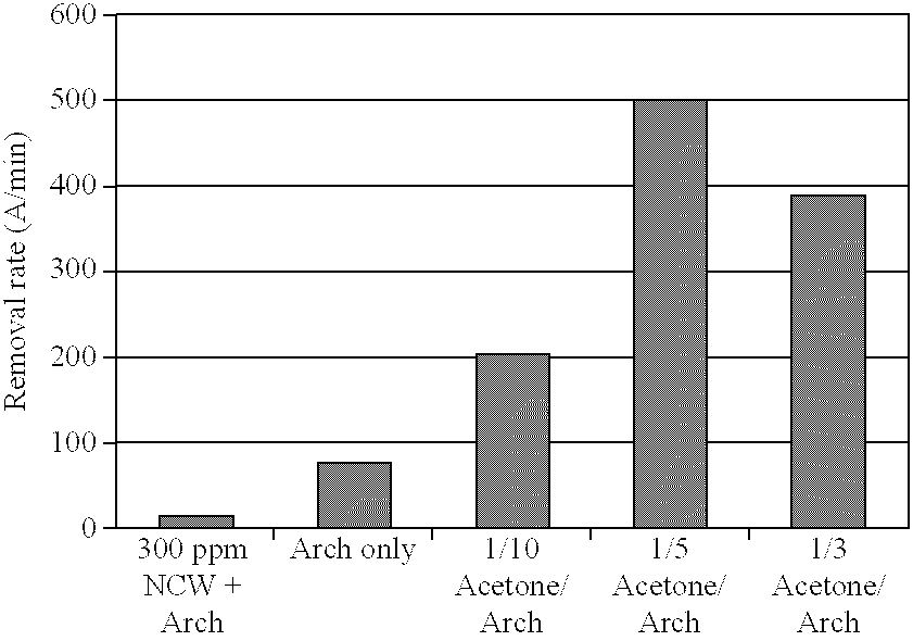
An example of an abrasive-free CMP composition described herein includes between about 0.1 vol % and about 1 vol % of polyethylene oxide or polyethylene oxide derivative, between about 0.3 vol % and about 3 vol % of ethylenediamine, between about 0.5 vol % and about 5.0 vol % hydrogen peroxide, between about 0.02 vol % and about 0.1 vol % benzotriazole, about 5 vol % isopropyl alcohol, phosphoric acid as a pH adjusting agent to produce a pH level between about 4 and about 8, and distilled water.

One example of an abrasive-free CMP process employs using the above described composition in the apparatus described above and shown in FIG. 1 by using a polishing pressure between about 1 and about 8 psi, and a platen speed between about 20 and about 120 rpm for a polishing duration between about 30 seconds and about 2,000 seconds to planarize a substrate.

FIGS. 2-4 are schematic diagrams illustrating one embodiment of a process for forming a feature on a substrate utilizing the invention des...


PUM


Abstract

A method and composition for planarizing a substrate. The composition includes one or more chelating agents, one or more oxidizers, one or more corrosion inhibitors, a polar solvent, and deionized water. The composition may further comprise one or more surfactants, one or more agents to adjust the pH and/or abrasive particles. The method comprises planarizing a substrate using a composition including a polar solvent.

Description

1. Field of the InventionThe invention relates generally to the fabrication of semiconductor devices and to polishing and planarizing of substrates.2. Background of the Related ArtReliably producing sub-half micron and smaller features is one of the key technologies for the next generation of very large scale integration (VLSI) and ultra large scale integration (ULSI) of semiconductor devices. However, as the fringes of circuit technology are pressed, the shrinking dimensions of interconnects in VLSI and ULSI technology has placed additional demands on the processing capabilities. The multilevel interconnects that lie at the heart of this technology require precise processing of high aspect ratio features, such as vias, contacts, lines, and other interconnects. Reliable formation of these interconnects is important to VLSI and ULSI success and to the continued effort to increase circuit density and quality of individual substrates and die.In order to further improve the current dens...

Claims


Application Information

Patent Timeline
IPC IPC(8): C09G1/00C09G1/04H01L21/321
CPCC09G1/04H01L21/3212
Inventor WANG, YUCHUNBAJAJ, RAJEEVREDEKER, FRED C.
Owner APPLIED MATERIALS INC
Why Eureka
Try Eureka