

Semiconductor device with varying thickness gold electrode
a technology of gold electrodes and semiconductor devices, which is applied in the direction of basic electric elements, lasers, semiconductor lasers, etc., can solve the problems of similar problems, difficult cleaving of devices, and expected to arise, and achieve the effect of avoiding similar problems and avoiding problems
- Summary
- Abstract
- Description
- Claims
- Application Information
AI Technical Summary
Problems solved by technology
Method used
Image

Examples
first embodiment
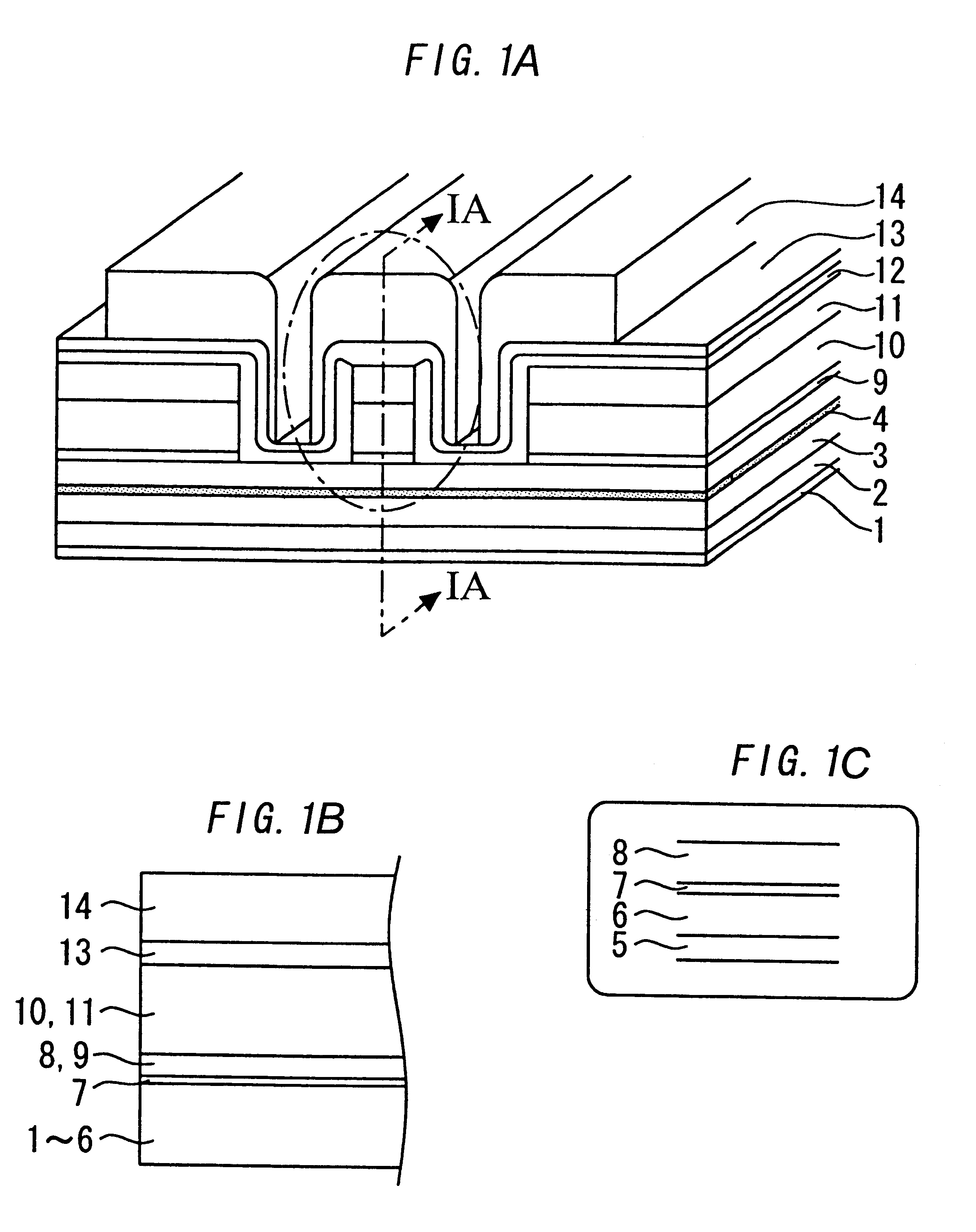
FIG. 1A is an illustration showing the structure of a semiconductor optical device according to the present invention. The semiconductor optical device shown in FIG. 1A is a ridge waveguide semiconductor laser manufactured through use of the known technique. A semiconductor substrate--on which a laser structure is formed through epitaxial growth--is of arbitrary conductivity type. The general characteristic of the present invention is not lost even when semiconductor material of arbitrary type (e.g., InP, GaAs, or Si) is used for a substrate or a laser structure.
For the sake of convenience, manufacturing processes will be described by taking, as an example, an AlGaInAs ridge laser formed on an n-InP substrate. First, an n-InP buffer layer 3 (having a thickness of 0.3 to 1.0 .mu.m) and an n-AlGaInAs BDR layer 4 (having a thickness of 0.05 to 0.1 mm) are formed through epitaxial growth, on an n-InP single crystal substrate 2 formed on the underside electrode 1.
An n-AlInAs optical conf...
second embodiment
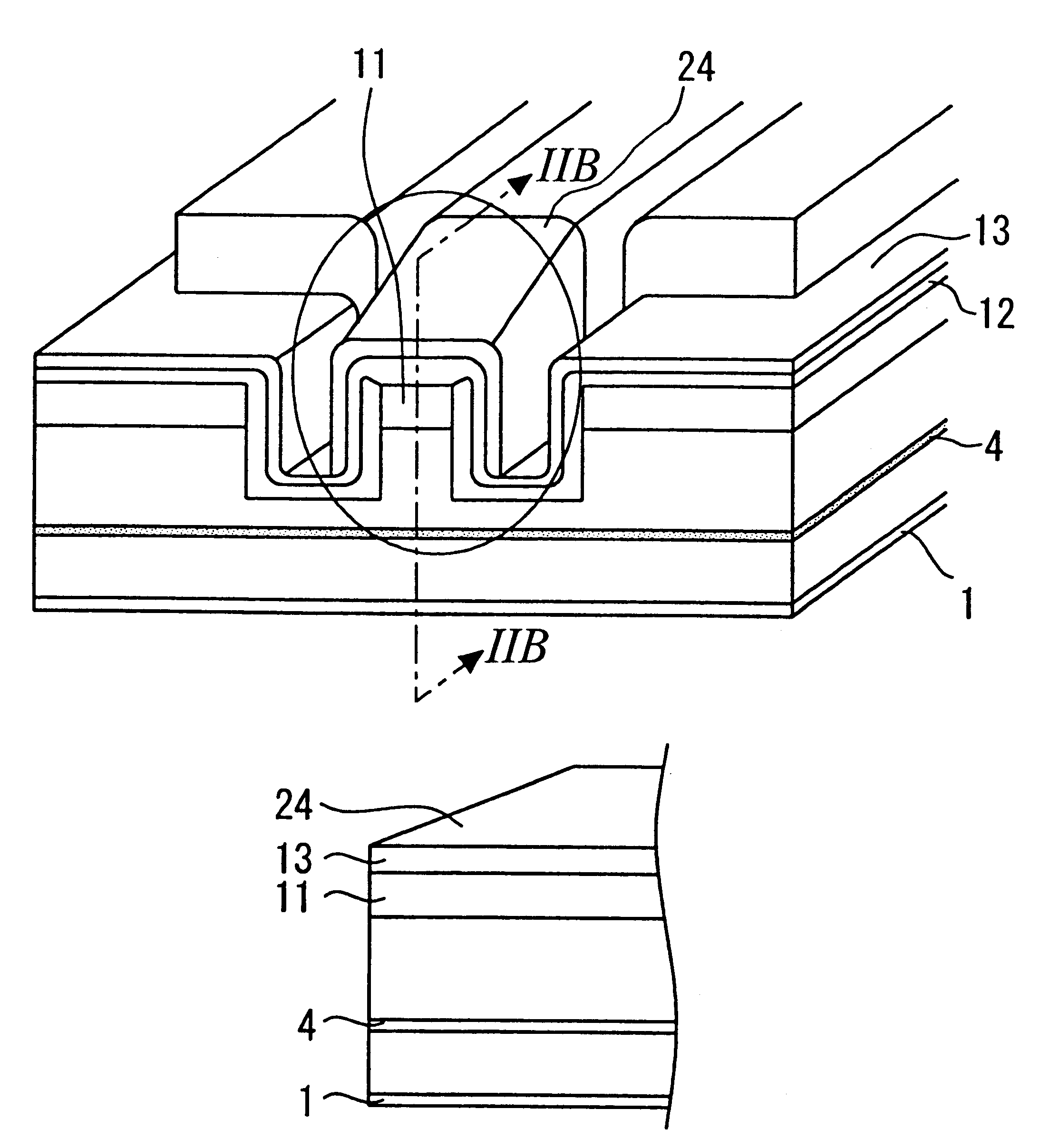
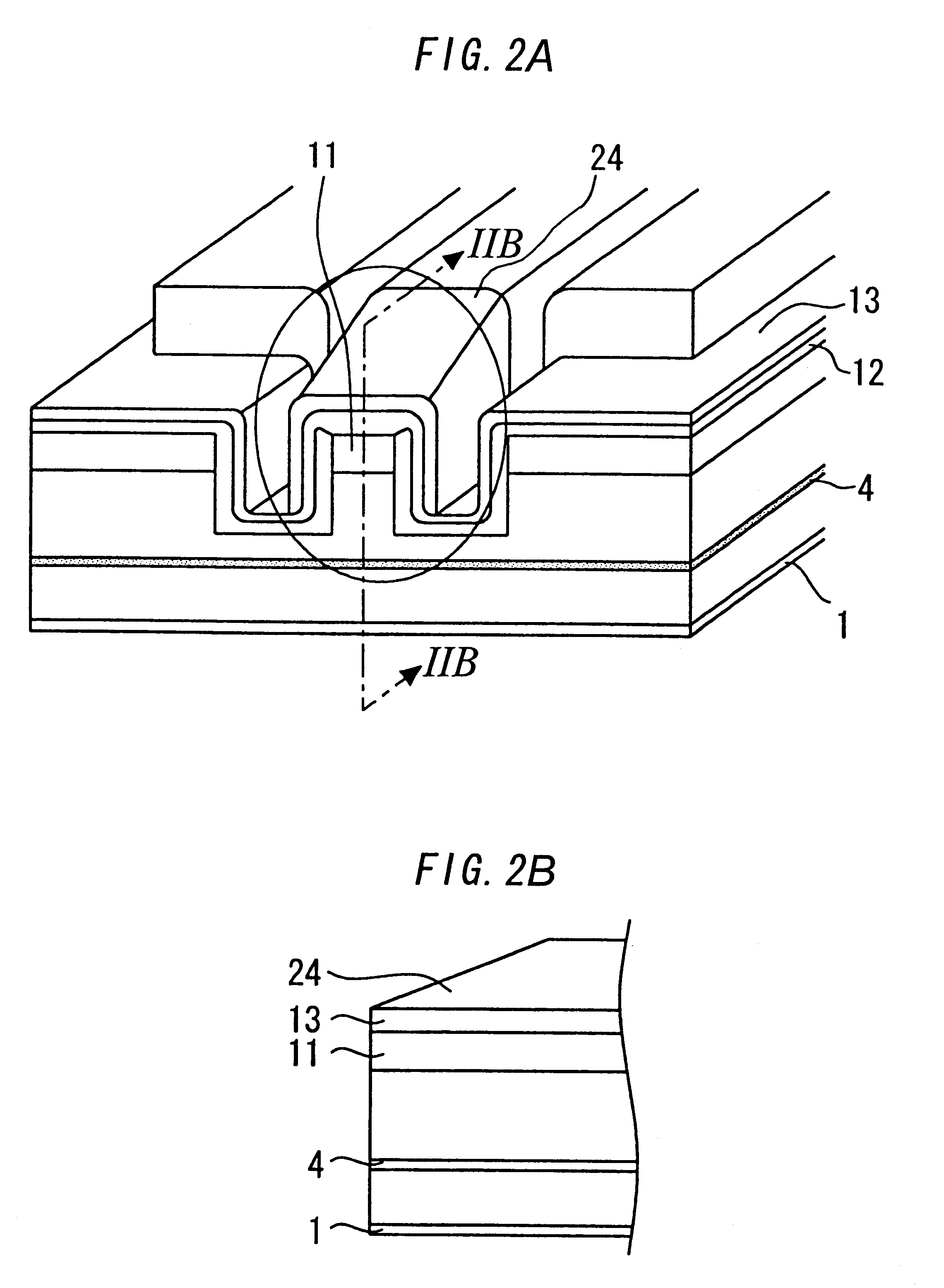
FIG. 2A is an illustration showing the structure of a semiconductor optical device according to a second embodiment of the present invention. FIG. 2B is a cross-sectional view taken along line IIB--IIB of FIG. 2. The semiconductor optical device shown in FIG. 2A is a ridge waveguide semiconductor laser manufactured through use of the known technique. Procedures through manufacture of an epitaxial wafer for a ridge laser and procedures through production of the thin gold film 13 are the same as those in the first embodiment, and repeated explanation thereof is omitted. In relation to the structure of the device, elements which are the same as those described in connection with the first embodiment are assigned the same reference numerals, and illustration of the elements is omitted. Only the area around the structure of gold plating is shown in detail.
Even in the second embodiment, gold plating 24 is deposited over the entire thin gold film 13. When the gold plating 24 is deposited o...
third embodiment
FIG. 3A is an illustration showing the structure of a semiconductor optical device according to a third embodiment of the present invention. FIG. 3B is a cross-sectional view taken along line IIIB--IIIB of FIG. 3A. The semiconductor optical device shown in FIG. 3A is a ridge waveguide semiconductor laser manufactured through use of the known technique. Procedures through manufacture of an epitaxial wafer for a ridge laser and procedures through production of the thin gold film 13 are the same as in the first and second embodiments, and repeated explanations thereof are omitted. In relation to the structure of the device, elements which are the same as those described in connection with the first and second embodiments are assigned the same reference numerals, and illustration of the elements is omitted. Only the area around the structure of gold plating is shown in detail.
In the third embodiment, first gold plating 14, which is thinner (having a thickness of, e.g., 150 nm or thereab...
PUM
| Property | Measurement | Unit |
|---|---|---|
| thickness | aaaaa | aaaaa |
| thickness | aaaaa | aaaaa |
| thickness | aaaaa | aaaaa |
Abstract
Description
Claims
Application Information