Fast method of I/O circuit placement and electrical rule checking

a fast method and circuit technology, applied in the field of analyzing the layout of i/o cells, can solve the problems of limit of placement of different types of i/o cells in the available locations, limit of test circuits, other limits on placement needed

Inactive Publication Date: 2003-06-24
IBM CORP
View PDF6 Cites 37 Cited by
  • Summary
  • Abstract
  • Description
  • Claims
  • Application Information

AI Technical Summary

Problems solved by technology

In practice, however, not all these locations are identical and there are limits to the placement of different types of I/O cells in the available locations.
Another limit relates to test circuits which can be placed only in special test circuit I/O cell slots.
There are other limits on placement needed to minimize electromigration and noise.
Any changes made late in the design process to this early proposed I/O cell layout increases cost.
The packaging may also put limits on the placement of the I/O cells on the silicon die.
With more I/O cells switching, total noise increases and it has become significantly more difficult to place I/O cells in a proposed I/O cell layout that is workable.
The increasing complexity of the on chip metal wiring has made manual IR drop calculations difficult, while the increasing frequencies of ASIC chips has made it important to decrease noise.
Although most ASIC designs are given a very comprehensive analysis of timing, test coverage, DRC and LVS, the electrical analysis of the power bus is very limited in scope.
Some ASIC designs continue to fail for reasons not predicted before the design is manufactured due to the limited scope of the power bus analysis.
Some of these failures have been traced to power supply compression resulting from resistive IR voltage drop and inductive di/dt noise caused by switching high speed I/Os.
Wh

Method used


Image

  • Fast method of I/O circuit placement and electrical rule checking
  • Fast method of I/O circuit placement and electrical rule checking
  • Fast method of I/O circuit placement and electrical rule checking

Examples


Embodiment Construction

)

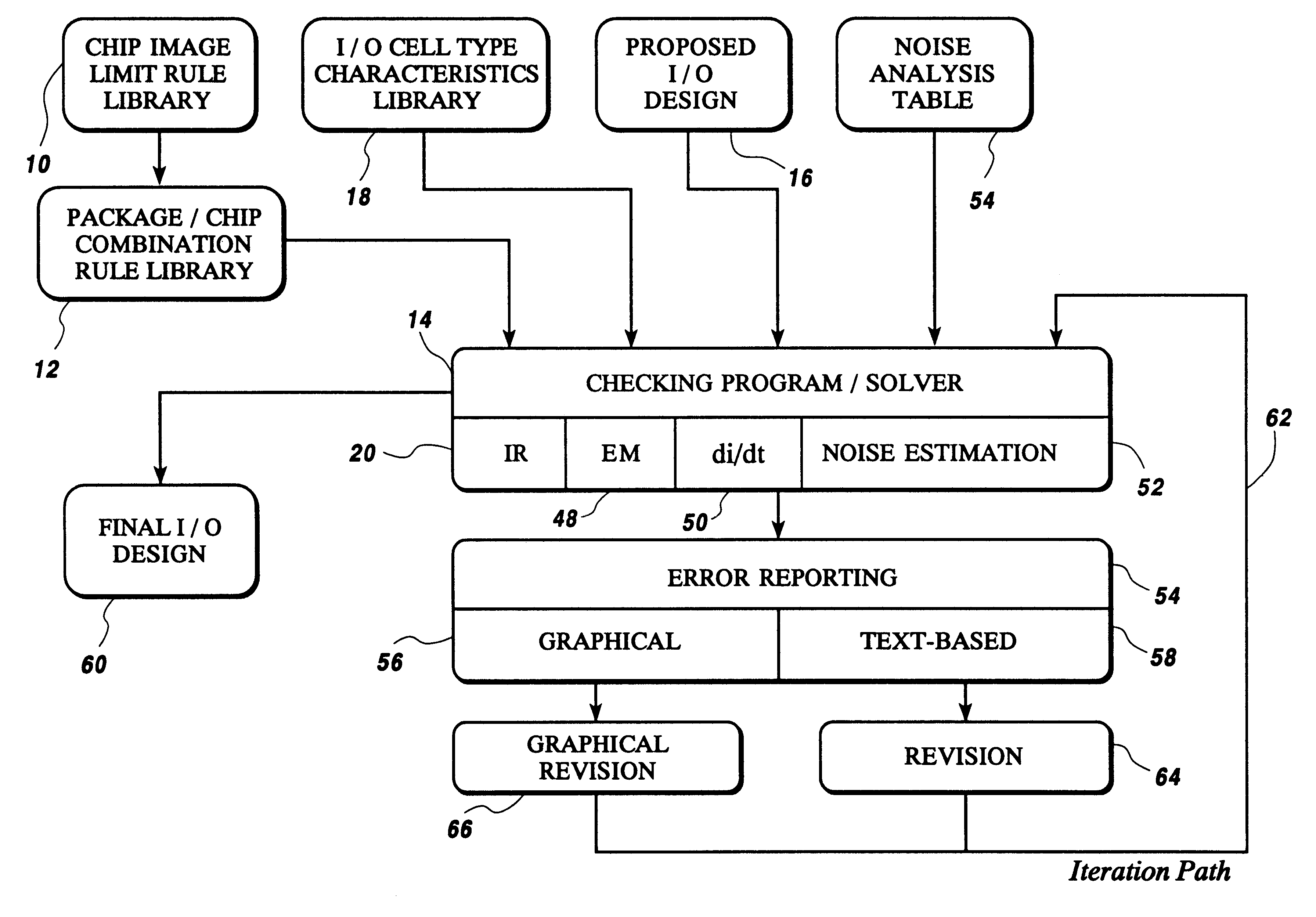
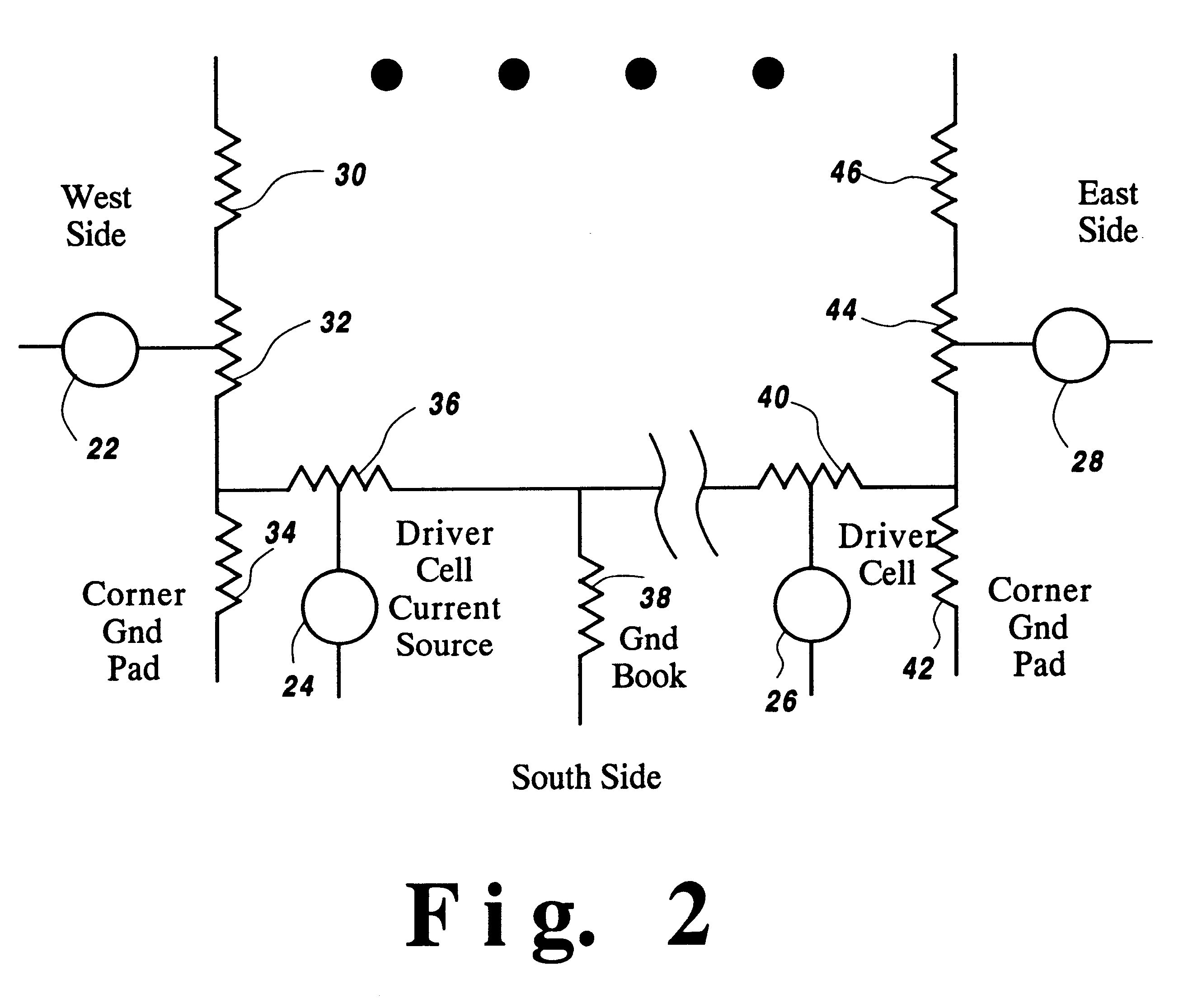
In describing the preferred embodiment of the present invention, reference will be made herein to FIGS. 1-2 of the drawings in which like numbers refer to like features of the invention. Features of the invention are not necessarily shown to scale in the drawings.

In order to understand the method of the present invention, a brief description of the design process is helpful. The present invention is described in connection with the design of a custom ASIC chip, but it is also applicable to design of other integrated circuits.

The ASIC chip designer knows the intended function of the ASIC and from this function is able to determine the required inputs and outputs to the chip at the beginning of the design process. The chip manufacturer provides a library of standard I / O cell types that the ASIC designer may use and a variety of silicon dies which differ in size and suitable packages for those dies on which the ASIC circuit, including the I / O cells, can be constructed. The designer se...


PUM


Abstract

A method of analyzing I/O cell layouts for integrated circuits, such as ASICs, includes defining a proposed I/O cell layout on a selected chip image, providing a set of limit rules for electromigration, IR voltage drop and di/dt noise for the selected chip image, providing characteristics for each I/O cell type used in the proposed I/O cell layout, checking the proposed I/O cell layout by applying the limit rules to the proposed I/O cell layout and reporting all I/O cells used in the proposed I/O cell layout that do not meet the limit rules for the selected chip image.

Description

1. Field of the InventionThis invention relates to methods of analyzing I / O cell layouts for integrated circuits, where the layout includes a location and type for each I / O cell used in the integrated circuit. More specifically, this invention relates to methods of analyzing a proposed I / O cell layout at an early stage in the design of an integrated circuit to determine whether the relative arrangement of the I / O cells and the particular types of I / O cells chosen for the layout will meet design goals with respect to power bus voltage drop, electromigration and noise limits.2. Description of Related ArtTo reduce cost and speed design, integrated circuits, such as custom logic application specific integrated circuits (ASIC) chips, are usually constructed from standard elements. These elements include such items as the die size for the silicon chip, the packaging, and the input / output (I / O) circuitry.Typically, each I / O circuit is selected by the integrated circuit designer from a libr...

Claims


Application Information

Patent Timeline
IPC IPC(8): G06F17/50
CPCG06F17/5036G06F30/367
Inventor CHIU, CHARLES S.LIBOUS, JAMES P.LOUGHRAN, RORY D.NATONIO, JOSEPHPROCTOR, ROBERT A.YASAR, GULSUN
Owner IBM CORP
Why Eureka
Try Eureka