Organic EL device
a technology of electroluminescent devices and organic el, which is applied in the direction of discharge tube luminescnet screens, other domestic articles, organic chemistry, etc., can solve the problems of difficult choice of host materials, failure of organic el devices to reach a practicable level of emission efficiency, and often failure of el devices to allow dopant molecules to exert their own fluorescen
- Summary
- Abstract
- Description
- Claims
- Application Information
AI Technical Summary
Problems solved by technology
Method used
Image
Examples
example 1
On a glass substrate, a transparent ITO electrode thin film was deposited to a thickness of 100 nm by RF sputtering and patterned. The glass substrate having the transparent ITO electrode was subjected to ultrasonic washing with neutral detergent, acetone, and ethanol, pulled up from boiling ethanol, and dried. The transparent electrode surface was further cleaned with UV / ozone. Thereafter, the substrate was secured by a holder in a vacuum evaporation chamber, which was evacuated to a vacuum of 1.times.10.sup.-5 Pa or lower.
With the vacuum kept, N,N'-diphenyl-N,N'-bis[N-(4-methylphenyl)-N-phenyl-(4-aminophenyl)]-1,1'-biphenyl-4,4'-diamine was evaporated at a deposition rate of 0.1 nm / sec. to a thickness of 50 nm, forming a hole injecting layer.
Then, N,N,N',N'-tetrakis(m-biphenyl)-1,1'-biphenyl-4,4'-diamine (TPD) was evaporated at a deposition rate of 0.1 nm / sec to a thickness of 20 nm, forming a hole transporting layer.
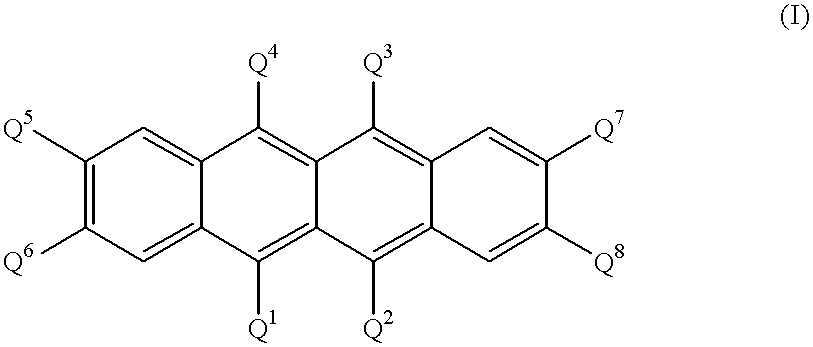
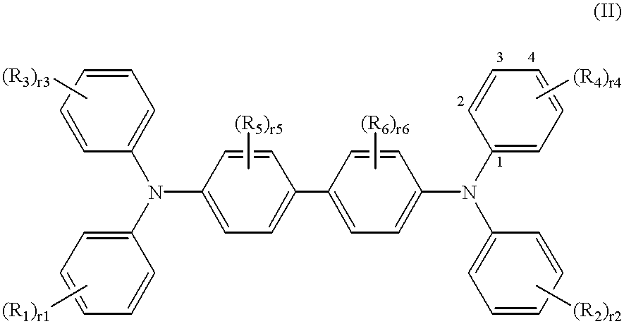
With the vacuum kept, the host material and dopant of the follow...
example 2
An organic EL device was prepared as in Example 1 except that the host material in the light emitting layer was changed to the following compound. ##STR4862##
A DC voltage was applied across the organic EL device. Initially, the device was found to produce light emission to a luminance of 504 cd / m.sup.2 when operated at a current density of 10 mA / cm.sup.2 and a drive voltage of 5.9 volts. The current efficiency was 5.0 cd / A, the power efficiency was 2.7 lm / W, the chromaticity coordinates (x, y) were (0.64, 0.36), and the maximum luminance was 11,500 cd / m.sup.2. When the device was continuously driven by conducting a constant current of 50 mA / cm.sup.2, it exhibited an initial luminance of at least 2,170 cd / m.sup.2 and a luminance half-life period of more than 1,500 hours.
example 3
An organic EL device was prepared as in Example 1 except that the host material in the light emitting layer was changed to the following compound. ##STR4863##
A DC voltage was applied across the organic EL device. Initially, the device was found to produce light emission to a luminance of 449 cd / m.sup.2 when operated at a current density of 10 mA / cm.sup.2 and a drive voltage of 5.9 volts. The current efficiency was 4.5 cd / A, the power efficiency was 2.4 lm / W, the chromaticity coordinates (x, y) were (0.66, 0.34), and the maximum luminance was 17,200 cd / m.sup.2. When the device was continuously driven by conducting a constant current of 50 mA / cm.sup.2, it exhibited an initial luminance of at least 2,440 cd / m.sup.2 and a luminance half-life period of more than 1,500 hours.
PUM
| Property | Measurement | Unit |
|---|---|---|
| voltage | aaaaa | aaaaa |
| luminance | aaaaa | aaaaa |
| luminance | aaaaa | aaaaa |
Abstract
Description
Claims
Application Information


