Method of reducing plasma charging damage during dielectric etch process for dual damascene interconnect structures

a dielectric etching and interconnecting technology, applied in the direction of basic electric elements, semiconductor/solid-state device manufacturing, electric apparatus, etc., can solve the problems of tunneling current which can do severe damage to the underlying layer, less able to penetrate the electrons in the plasma to the bottom of the etched feature, and worsening the electron shading

Inactive Publication Date: 2003-09-02
APPLIED MATERIALS INC
View PDF13 Cites 36 Cited by
  • Summary
  • Abstract
  • Description
  • Claims
  • Application Information

AI Technical Summary

Problems solved by technology

This serves to accelerate positively-charged species toward the target surface, but leaves the electrons in the plasma less able to penetrate to the bottom of the etched feature.
When the resultant positive charge near the bottom of the feature becomes sufficiently high, it results in a tunneling current which can do severe damage to underlying layers.
The electron shading effect gets worse as the aspect ratio increases, since the electron accumulation near the opening and top sidewalls of the feature makes it increasingly difficult for anything but the positively charged high energy species to get past that entrance and any distance down into the deepening etched feature.
Electron shading effects are often a serious problem during fabrication of dual damascene structures.

Method used


Image

  • Method of reducing plasma charging damage during dielectric etch process for dual damascene interconnect structures
  • Method of reducing plasma charging damage during dielectric etch process for dual damascene interconnect structures
  • Method of reducing plasma charging damage during dielectric etch process for dual damascene interconnect structures

Examples


Embodiment Construction

of the Method

In the present invention, charging damage to a semiconductor structure, caused by electron shading during plasma etching in a dual damascene structure, is alleviated by first depositing a protective conductive layer which provides a conductive path for maintaining charge balance in the etched structures. This conductive layer reduces the buildup of unbalanced positive charge in the contact opening, and consequently the damage done to underlying layers by the resultant tunneling current.

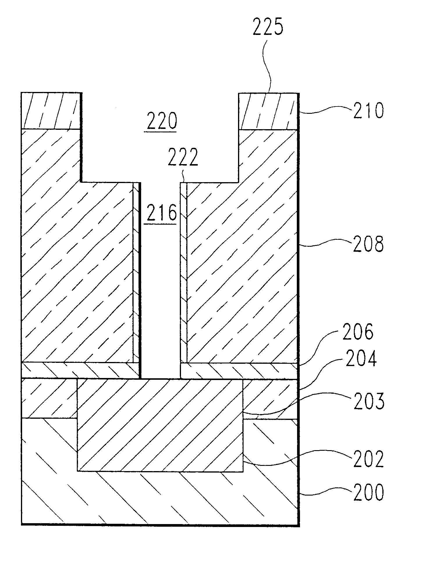
The starting structure for this illustrative embodiment of the present invention is as shown in FIG. 2A in which a conductor 202, such as copper or aluminum or alloys thereof, is embedded in a dielectric 200, an upper portion of the conductor is contacted at sidewall 203 by a layer of a first dielectric hardmask 204, and an upper surface 205 of dielectric hardmask layer 204 and an upper surface 207 of conductor 202 are both covered by an etch stop layer 206, typically a dielectric such as...


PUM


Abstract

Charging damage, caused by electron shading during plasma etching in a dual damascene structure, is alleviated by first depositing a protective conductive layer which provides a conductive path for maintaining charge balance in the etched structures. This conductive layer reduces the buildup of unbalanced positive charge in the contact opening, and the damage done to underlying layers caused by the resultant tunneling current. Further, if the protective conductive layer comprises a material which can also serve as an interdiffusion barrier layer for the contact opening fill material, a separate subsequent step to deposit such a barrier layer on the contact opening sidewall is avoided. Further, in the process of doing lithography on the trench etch resist layer, the protective conductive layer also functions as an antireflective coating, permitting the stepper to accurately focus the desired pattern.

Description

1. Field of the InventionThe present invention relates to the alleviation of charge buildup on integrated circuit components during dry plasma etching of semiconductor interconnect feedthrough structures.2. Brief Description of the Background ArtIn the quest for ever-higher circuit densities in modem very large scale integrated circuit semiconductors, engineers have moved from conventional chip layouts, in which interconnects between active regions on the chip are formed by metallic, generally aluminum, conductors in the plane of the devices, connected layer-to-layer mostly at the outer edges, to dual damascene architecture. In a dual-damascene structure, multiple layers of active devices are separated by layers of dielectric material, which are traversed within a given layer by trenches filled with conductive materials, which in turn are connected layer-to-layer by interconnects formed by filling through-openings with conductive materials. These contact openings, typically referred...

Claims


Application Information

Patent Timeline
Patent Type & Authority Patents(United States)
IPC IPC(8): H01L21/768H01L21/70
CPCH01L21/76808H01L21/76831H01L21/76843H01L21/76844
Inventor MA, SHAWMING
Owner APPLIED MATERIALS INC
Why Eureka
Try Eureka