Method and apparatus for biasing selected and unselected array lines when writing a memory array

a memory array and array line technology, applied in the field of semiconductor memory arrays, can solve the problems of cmos latchup event, large chip area required by such on-chip circuitry to generate programming voltage sources with sufficient current capability to support unselected memory cells,

Inactive Publication Date: 2003-09-09
SANDISK TECH LLC
View PDF31 Cites 217 Cited by
  • Summary
  • Abstract
  • Description
  • Claims
  • Application Information

AI Technical Summary

Benefits of technology

By removing the V.sub.PP generator, a higher value for V.sub.PP may be used with the same semiconductor process, which allows much faster programming. Alternatively, for a given voltage necessary to program a particular memory cell technology, the overall voltage requirements of the semiconductor technology may be relaxed. This may allow an even greater savings in integrated circuit area, as the spacing between various on-chip structures may be reduced. Preferably, the programming voltage received from an external voltage source is the highest voltage conveyed anywhere in the chip, and other bias voltages may either be received from other external voltage sources or generated using on-chip circuitry.
When discharging the memory array, the capacitance between layers (i.e., between memory array lines on adjacent layers), in particular the substantial capacitance from the unselected Y-lines to adjacent unselected X-lines, is preferably discharged first by driving their X-lines and Y-lines to nearly the same voltage. The array lines may then be safely discharged to ground without coupling array lines on adjacent layers below ground and potentially causing a CMOS latchup event to occur.
The invention is particularly applicable to a passive element array having an antifuse and diode in series as the memory element, but is also applicable to other passive element memory arrays. Other preferred embodiments are provided, and each of the preferred embodiments described herein can be used alone or in combination with one another.

Problems solved by technology

Integrated circuits incorporating a passive element memory array require a high-voltage and high-current programming voltage source due to the large number of leakage paths in the array and the high voltage required to program the element conductivity.
The leakage current represents a significant portion of the power dissipation of such circuits during programming.
However, the chip area required by such on-chip circuitry to generate the programming voltage source with enough current capability to support the leakage current of unselected memory cells is substantial.
The array lines may then be safely discharged to ground without coupling array lines on adjacent layers below ground and potentially causing a CMOS latchup event to occur.

Method used


Image

  • Method and apparatus for biasing selected and unselected array lines when writing a memory array
  • Method and apparatus for biasing selected and unselected array lines when writing a memory array
  • Method and apparatus for biasing selected and unselected array lines when writing a memory array

Examples


Embodiment Construction

)

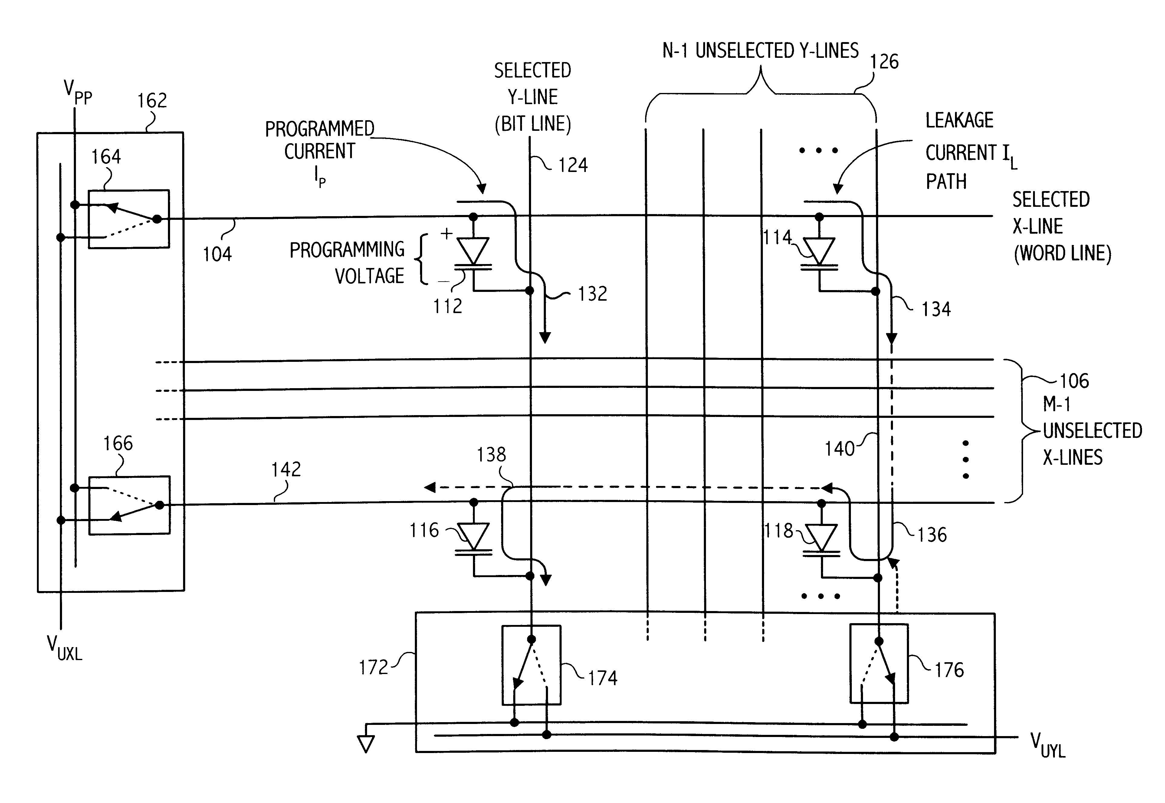
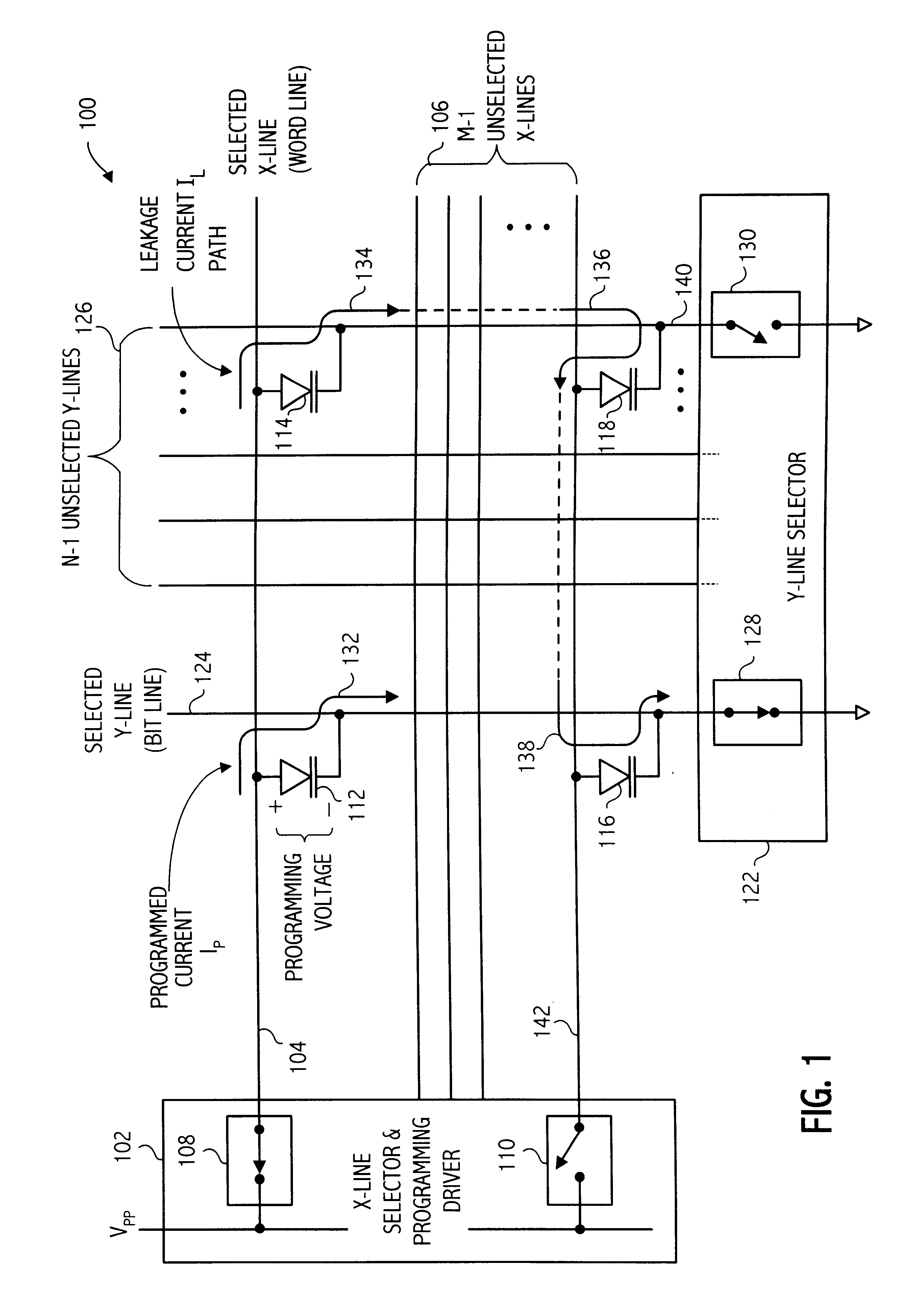
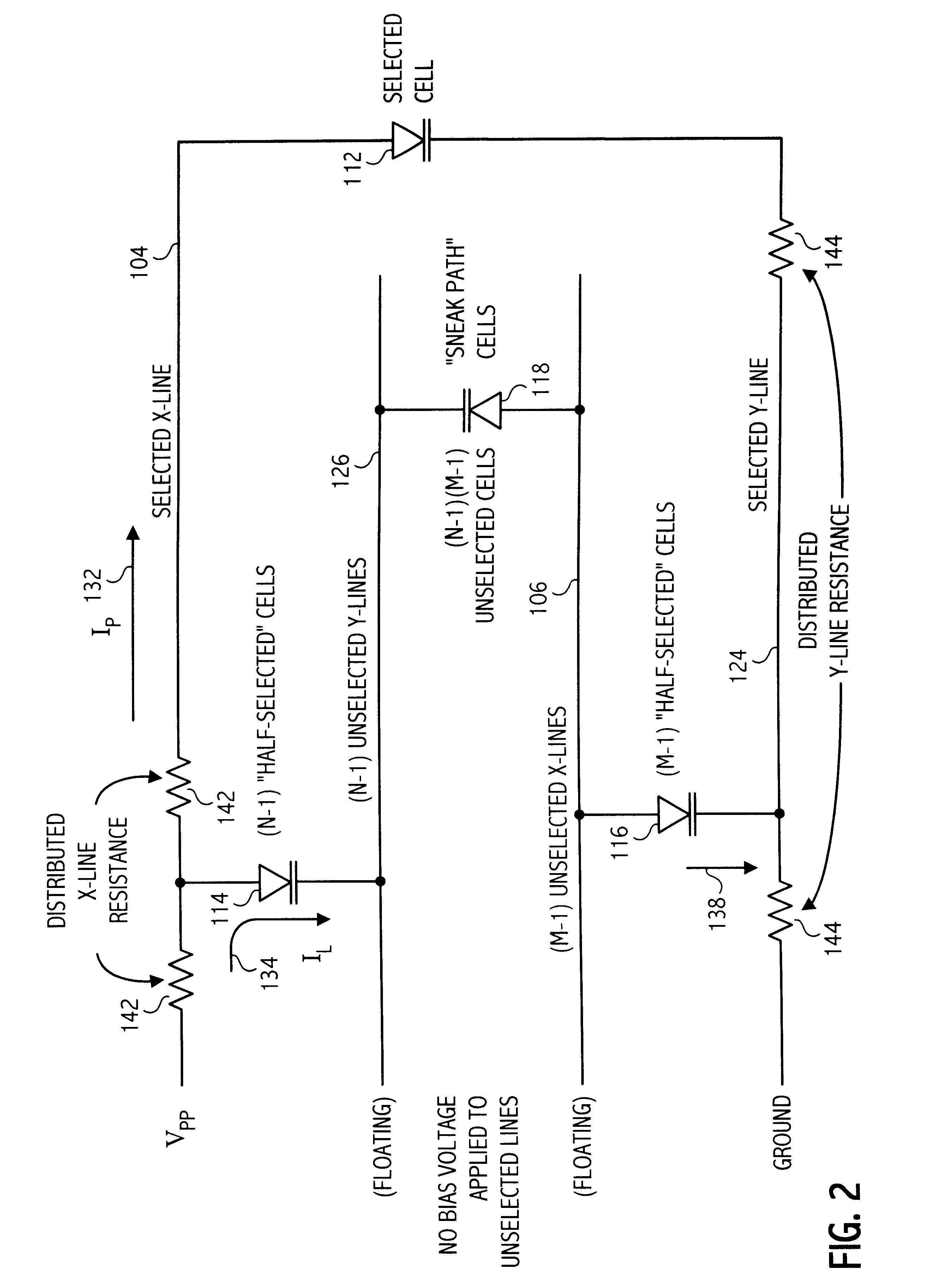
For passive element memory arrays, a high voltage V.sub.PP (also variously known as and described herein as V.sub.P or as V.sub.PROG) is applied across a memory cell within the memory array to program the conductivity of the memory cell. In a write mode of operation, for example, one word line may be raised to a positive voltage and one bit line may be held at ground. It is necessary to apply the V.sub.PP to just a selected memory cell, but not to other memory cells that are also connected to the selected word line and bit line.

Referring now to FIG. 1, a memory array 100 is shown which utilizes passive element memory cells. Each passive element memory cell is generally a two-terminal memory cell having a steering element in series with a state change element, together connected between one of M possible X-lines (i.e., word lines) and one of N possible Y-lines (i.e., bit lines). These two elements within a memory cell may both be present before programming. Alternatively, the steeri...


PUM


Abstract

A passive element memory array preferably biases selected X-lines to an externally received VPP voltage and selected Y-lines to ground. Unselected Y-lines are preferably biased to VPP minus a first offset voltage, and unselected X-lines biased to a second offset voltage (relative to ground). The first and second offset voltages preferably are identical and have a value of about 0.5 to 2 volts. The VPP voltage depends upon the memory cell technology used, and preferably falls within the range of 5 to 20 volts. The area otherwise required for an on-chip VPP generator and saves the power that would be consumed by such a generator. In addition, the operating temperature of the integrated circuit during the programming operation decreases, which further decreases power dissipation. When discharging the memory array, the capacitance between layers is preferably discharged first, then the layers are discharged to ground.

Description

1. Field of the InventionThe present invention relates to semiconductor memory arrays, and particularly to three-dimensional passive element memory arrays.2. Description of the Related ArtIntegrated circuits incorporating a passive element memory array require a high-voltage and high-current programming voltage source due to the large number of leakage paths in the array and the high voltage required to program the element conductivity. The leakage current represents a significant portion of the power dissipation of such circuits during programming. There remains a need for improved performance of such circuits, reduced leakage currents when writing, and faster write time of a selected memory cell.An improved passive element memory array biases unselected X-lines to one voltage, and biases unselected Y-lines to another voltage, both having a value less than the programming voltage. In a preferred embodiment, four voltage levels are applied to the array to bias the array for write mo...

Claims


Application Information

Patent Timeline
Patent Type & Authority Patents(United States)
IPC IPC(8): G11C8/08G11C5/02G11C7/18G11C8/00G11C7/06G11C7/00G11C8/10G11C17/18G11C17/16G11C17/14
CPCG11C5/025G11C7/062G11C7/067G11C7/18G11C8/08G11C8/10G11C13/0023G11C13/0028G11C13/0069G11C17/16G11C17/18G11C2013/0092G11C2207/063G11C2213/72G11C2213/73
Inventor SCHEUERLEIN, ROY E.
Owner SANDISK TECH LLC
Why Eureka
Try Eureka