
Electronic and optical devices and methods of forming these devices

a technology of optical devices and electronic devices, applied in the direction of fixed capacitor details, waveguides, instruments, etc., can solve the problems of affecting the designability of radio frequency (rf) or electrooptic devices, affecting the freedom of designability of radio frequency or electrooptic devices, etc., to minimize the interaction with wave propagation, minimize loss, and minimize leakage

Inactive Publication Date: 2006-12-05
NGIMAT CO
View PDF5 Cites 10 Cited by
  • Summary
  • Abstract
  • Description
  • Claims
  • Application Information

AI Technical Summary

Benefits of technology

[0023]Very thin layers of various materials can meet this objective. Also, materials which are mixed conductors, that is electronic and ionic, or more likely ionic or semi-conducting, thus aiding in the modulation of further resistance at higher frequencies while still allowing enough conductivity at low frequencies or DC voltages to enable biasing of the ferroelectric materials while minimizing the effect on the performance of the device. Conductors have distinct amounts of carriers and mobilities. The carriers can be electrons, holes or a mixture thereof. Of benefit to this application, is reduced mobilities, in particular at the desired use frequency. A larger proportion of hole conductors can also benefit the RF / DC differential.
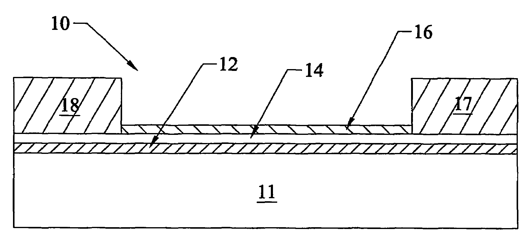
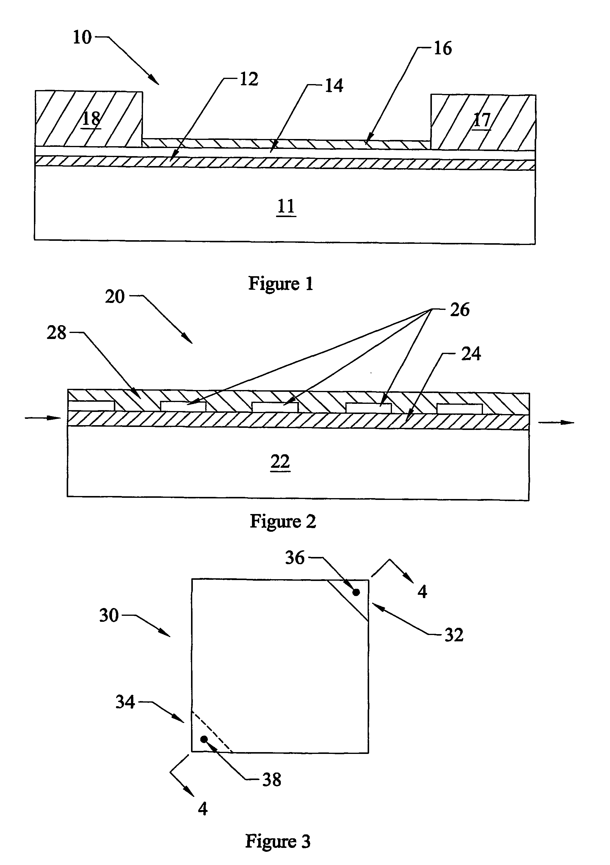
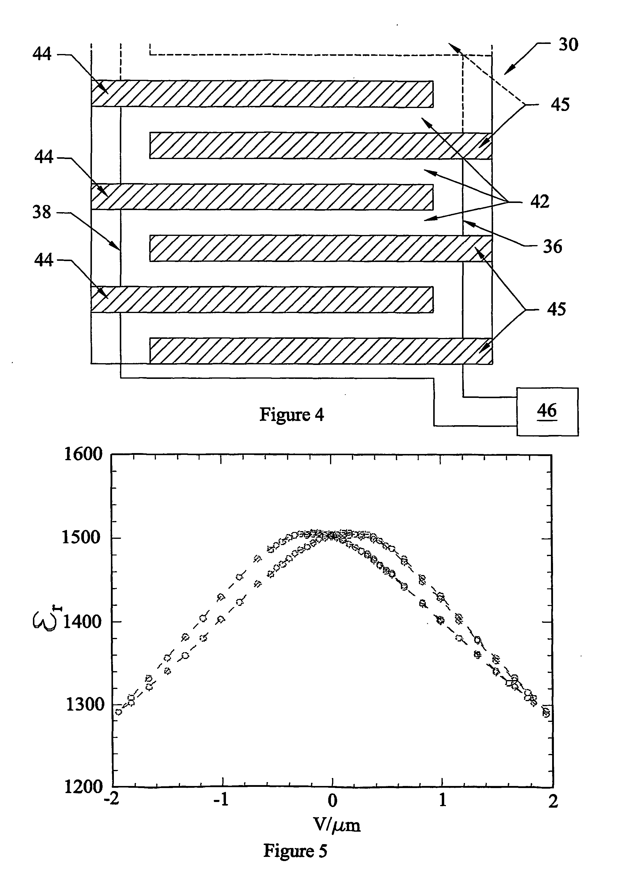
[0024]Any loss that is caused by the biasing electrodes is offset by the benefit to the system wherein the use of higher voltages as well as enabling the optimal, functional, device design including conductor separation. The materials of the biasing electrodes can be grown as a base layer (potentially epitaxial) prior to the variable dielectric material or they can be grown on top of the dielectric material or otherwise deposited thereon to form the system. To further minimize loss, the material can be discontinuous in design, so it is not a full sheet but has fine lines in various patterns. To further minimize the interaction with the wave propagation between the electrodes, the biasing electrodes can be formed as strips that are diagonal to the main electrodes (system lines), parallel to the system lines, or perpendicular to the system lines. The top and bottom bias strips can be directly across the thin film, or alternating. Alternating the bias strips will minimize leakage and can better align dielectric changes with some devices, but this can also slightly increase the bias voltage needed. The highly conductive main electrode device lines can be on one surface of the dielectric material film, with the bias voltage being applied between a main electrode that is electrically connected to one of the bias electrodes, and the biasing electrode on the other side of this thin film variable dielectric material. Alternatively, one device line can be contacting and used to apply the potential to one bias electrode and another device line can contact and be used to apply the potential to the other bias electrode thereby applying the net potential across the variable dielectric. Using the highly conductive device lines to apply the potential to shorter, more resistive bias electrodes will increase the speed of change in the variable dielectric, resulting in faster device speeds. The non-RF bias electrodes can also be deposited on only one surface and be formed as interdigital electrodes.
[0026]In the present invention, the phenomenon of intermodulation distortion is addressed by increasing the gap between the RF electrodes, thereby reducing the intensity of the RF-induced fields in the ferroelectric materials, and maintaining the dielectric constant of the materials approximately invariant to RF field strength. However, the DC tuning voltage is maintained low by extending highly resistive protrusions of material into the space between the RF electrodes. These protrusions are preferentially electrically connected to the RF electrodes themselves. Since the ferroelectric material presents a low-impedance path to the RF signals, the highly resistive protrusions will not significantly change the RF impedance of the overall structure. However, if a DC bias is applied to the RF electrodes in addition to the RF signal, the ferroelectric material will present a high impedance path to the DC signal, ideally forcing the protrusions to charge up to the DC voltage. If the spacing between the protrusions is small, this DC voltage will result in high electric field intensities in the ferroelectric material, and thereby effect tuning at low applied DC voltages. Since the value of the variable capacitor taught herein is independent of the intensity of the RF signal, while simultaneously is sensitive to small values of DC voltage, the problem of intermodulation distortion is greatly reduced.
[0027]In another aspect of the present invention, electrooptic or high index of refraction materials are deposited between two layers of material having lower indexes of refraction to form waveguides or optical filters. When the high index of refraction material is also electrooptic, the waveguide is steerable and the optical filter is tunable. In the steerable / controllable waveguide application, the use of the thin films of the present invention allows for preferable use of conductive oxides to act as the biasing electrodes, thereby eliminating the need for a cladding buffer layer and increasing the effectiveness of the waveguide. The use of TCOs together with electrooptical material allows the formation of a stack of high index of refraction and low index of refraction materials that can be tuned to allow modulation, switching, actuation, polarization or transmission of a particular wavelength of light. In this manner, the biasing voltage can be adjusted to control a number of aspects of the light.
[0028]In the case of photonics, the electrodes can be materials that might actually couple strongly with the light (if thick). For instance, metals and doped metals can be used, if thin enough to have only enough conductivity to enable biasing, but too thin to interact with the light. Semiconductors can also be used in many cases, as some of these materials are opaque in the visible range but transparent at infrared (IR) wavelengths. Silicon is one example of such a material that can be used as the dielectric in an optical stack type of filter described below. Other materials can be used as well, such as semiconductors, hole conductors, ionic conductors or mixed conductors. The objective of using these materials being to free the overall design to beyond transparent conductive oxides, TCOs and thereby enable materials that might be more compatible or easier to produce in the overall stack. The stack, preferably, having reduced or no grain boundaries. Furthermore, these materials can be more readily post processed or easier to manage in the deposition process.
[0029]Materials that have a larger variation in index of refraction such as plain silica for a low index material, can have added benefits. The materials next to the variable dielectric can be internally reflecting or transmitting layers. The bias voltage could be such that at some locations the adjacent materials cause the light to transform from internally reflecting to transmitting due to an index of refraction change in the material, thereby enabling a gate to open for the photons to pass through the waveguide device.

Problems solved by technology

This results in a change of capacitance or electromagnetic wave transmission between two main terminals also attached or in close proximity to the variable material.
The device conductors are used versus adding additional conductors to apply the bias because additional traditional conductors would affect the device performance.
This creates a limit due to the dimensional tolerance of manufacturing systems for imaging and etching.
In addition, the freedom of designability of the radio frequency (RF) or electrooptic (E-O) device is hampered by this need to keep the main conductors very close.
Additional designability issues preclude certain pattern due to the enhancement of electric fields (e.g. corners, acute angles) and the potential for premature breakdown.

Method used


Image

  • Electronic and optical devices and methods of forming these devices
  • Electronic and optical devices and methods of forming these devices
  • Electronic and optical devices and methods of forming these devices

Examples


example 1

Deposition of BST on Sapphire

[0085]In this example, Ba0.6Sr0.4TiO3 coatings were deposited onto C-plane Sapphire 250 nanometers thick using the CCVD process. The solution of the Ba0.6Sr0.4TiO3 precursor contained 0.0143 wt % of Sr in the form of strontium 2-ethylhexanoate, 0.0615 wt % of Ba in the form of barium 2-ethylhexanoate, 0.0355 wt % Ti (di-i-propoxide) bis (acetylacetonate), 12.6049 wt % toluene, 0.0118 wt % isoproponal, 1.5333 wt % 1-butanol, and 85.7412 wt % propane. The constant flow rate for the solution was at 2.0 ml / min and for the tip oxygen 4000 ml / min at 80 psi. The gas temperature as measured close to the substrate front surface varied from 900 to 1100° C. BST deposition was epitaxial with 1,1,1 lattice structure.

example 2

Deposition of BST on Sapphire and Device Construction

[0086]In this example, Ba0.6Sr0.4TiO3 coatings were deposited onto C-plane Sapphire 377 nanometers thick using the CCVD process. The solution of the Ba0.6Sr0.4TiO3 precursor contained 0.0143 wt % of Sr in the form of strontium 2-ethylhexanoate, 0.0615 wt % of Ba in the form of barium 2-ethylhexanoate, 0.0355 wt % Ti (di-i-propoxide) bis (acetylacetonate), 12.6049 wt % toluene, 0.0118 wt % isoproponal, 1.5333 wt % 1-butanol, and 85.7412 wt % propane. The constant flow rate for the solution was at 3.0 ml / min and for the tip oxygen 4000 ml / min at 80 psi. The gas temperature as measured close to the substrate front surface was 1200° C. Deposition was epitaxial with 1,1,1 lattice structure.

[0087]After forming the BST layer, a chromium bond layer and a gold conductive layer were formed on top of the BST using conventional coating methods. The chromium and gold were then patterned to form two electrodes of a 50 finger interdigital capaci...

example 3

[0091]In this example, Ba0.6Sr0.4TiO3 coatings were deposited onto polycrystalline alumina using the CCVD process. Polycrystalline alumina is a less expensive substrate material, but prior art techniques to deposit BST on alumina have resulted in significantly lower performance. By using CCVD, a quality layer was formed. The solution of the Ba0.6Sr0.4TiO3 precursor contained 0.0143 wt % of Sr in the form of strontium 2-ethylhexanoate, 0.0615 wt % of Ba in the form of barium 2-ethylhexanoate, 0.0355 wt % Ti (di-i-propoxide) bis (acetylacetonate), 12.6049 wt % toluene, 0.0118 wt % isopropanol, 1.5333 wt % 1-butanol, and 85.7412 wt % propane.

[0092]The constant flow rate for the solution was at 5.0 ml / min and for the tip oxygen 4020 ml / min at 30 psi. The gas temperature as measured close to the substrate front surface was 1150° C.


PUM

PropertyMeasurementUnit
thickaaaaaaaaaa
thickaaaaaaaaaa
thicknessaaaaaaaaaa

Abstract

Electronic and optical (or photonic) devices with variable or switchable properties and methods used to form these devices, are disclosed. More specifically, the present invention involves forming layers of conductive material and dielectric material or materials with varying conductivity and indexes of refraction to form various electronic and optical devices. One such layer of adjustable material is formed by depositing epitaxial or reduced grain boundary barium strontium titanate on the C-plane of sapphire.

Description

[0001]The present invention is directed to electronic and optical (or photonic) devices with variable or switchable properties and methods used to form these devices. More specifically, the present invention involves forming layers of conductive material and dielectric material or materials with varying conductivity and indexes of refraction to form various electronic and optical devices.BACKGROUND OF THE INVENTION[0002]Thin films (and thick films in some cases) are useful for forming many different electronic and optical devices. Capacitors (and other devices such as phase shifters) are formed by depositing dielectric material and conductive material layers, the conductive layer(s) forming the electrodes of the capacitor. In optical devices, films of material having relatively high indexes of refraction are deposited adjacent to films of materials having relatively low indexes of refraction to form wave-guides, filters, lenses and other devices. Many materials are useful for formin...

Claims


Application Information

Patent Timeline
Patent Type & Authority Patents(United States)
IPC IPC(8): H01P5/04G02B6/12G02B6/34G02F1/03G02F1/035G02F1/05G02F1/055G02F1/29H01G4/008H01G4/33H01G5/16H01G7/06H01L21/316H01L27/01H01P1/18
CPCG02B6/12004G02B6/12007G02B6/29361G02B6/29395G02F1/035G02F1/0508G02F1/0553H01G4/008H01G4/1227H01G4/33H01G7/06H01L27/016H01P1/181G02F1/0316G02F1/292H01L21/31691H01L21/02197
Inventor HUNT, ANDREW T.ALLEN, MARK G.KIESLING, DAVIDSCHWERZEL, ROBERT E.JIANG, YONGDONGGLADDEN, FE ALMAWEGMAN, JOHNZHAO, ZHIYONGVINSON, MATTHEW SCOTTMCENTYRE, J. ERICFLANAGAN, SCOTTPOLLEY, TODDKENNEY, J. STEVENSON
Owner NGIMAT CO
Learn More