Method for optimizing the planarizing length of a polishing pad

a polishing pad and planarizing technology, which is applied in the direction of lapping machines, manufacturing tools, abrasive surface conditioning devices, etc., can solve the problems of uneven surface on the wafer surface, uneven surface on the wafer, oxide layer pitting, etc., and achieve uniform decrease of the distance between the trenches on the first side of the polishing pad

Inactive Publication Date: 2003-09-16
APPLIED MATERIALS INC
View PDF25 Cites 50 Cited by
  • Summary
  • Abstract
  • Description
  • Claims
  • Application Information

AI Technical Summary

Problems solved by technology

When raw silicon wafers are manufactured, they commonly have surface irregularities on the wafer surface as a result of the manufacturing process.
However, the unevenness must be smoothed out without smoothing out the irregularities in the silicon, which are reproduced at the oxide surface.
Smoothing out the irregularities on the wafer surface will result in the oxide layer pitting and the wafer being unusable.
However, the hard abrasive material has a tendency to scratch wafers, and is also expensive.

Method used


Image

  • Method for optimizing the planarizing length of a polishing pad
  • Method for optimizing the planarizing length of a polishing pad
  • Method for optimizing the planarizing length of a polishing pad

Examples


Embodiment Construction

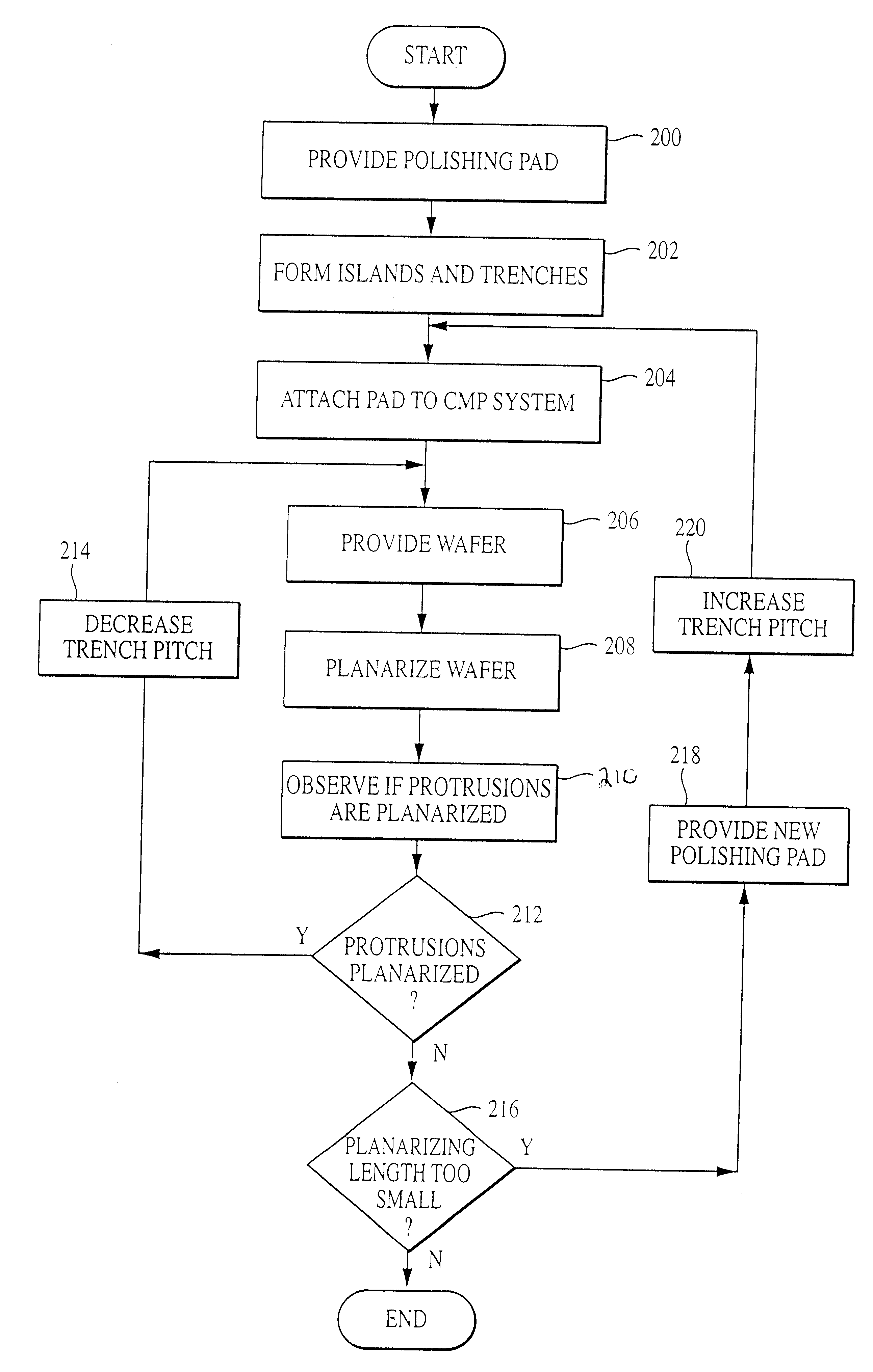
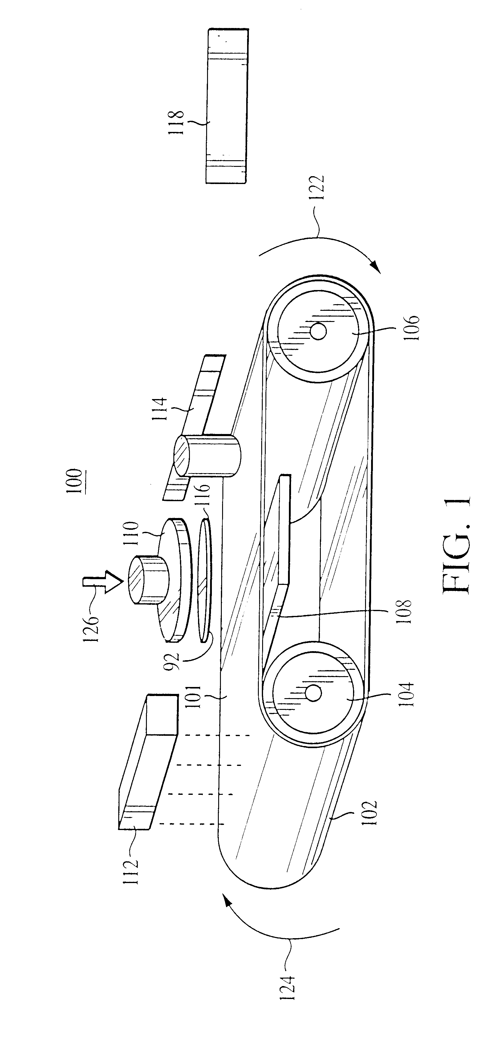
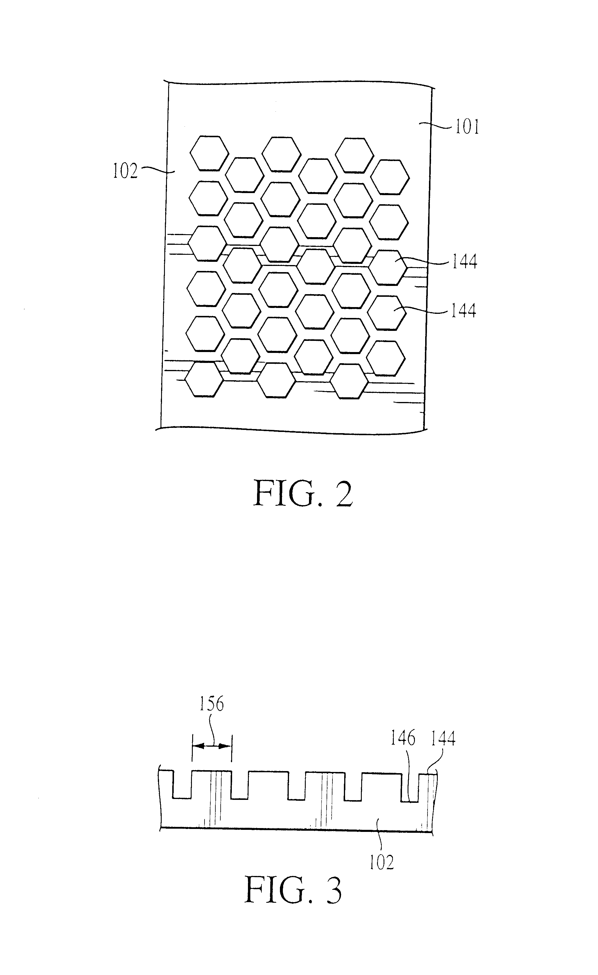
By way of introduction, FIG. 1 illustrates a linear chemical mechanical polishing or planarization (CMP) system 100 for polishing a workpiece. The system 100 includes a polishing pad 102 having a polishing surface 101, a first roller 104, a second roller 106, a platen 108, a polishing head 110, a slurry dispenser 112, a conditioner 114, and a controller 118. The system 100 in the illustrated embodiment is adapted for the planarization of wafers such as the semiconductor wafer 116.

As shown in FIG. 5, the semiconductor wafer 116 includes uniformly spaced peaks 90 that protrude outwardly from the wafer 116, a film surface layer 92, and a bottom layer 93. The film surface layer 92 preferably is an oxide film that is deposited over the bottom layer 93. Film layer 92 has features 94 that are the result of conforming to the shape of bottom layer 93 when it is deposited over bottom layer 93. Although a preferred embodiment includes a semiconductor wafer having an oxide film, the operative p...


PUM

PropertyMeasurementUnit
thicknessaaaaaaaaaa
thicknessaaaaaaaaaa
thicknessaaaaaaaaaa

Abstract

A method for optimizing the planarizing length of a polishing pad is disclosed that includes forming a substantially constant network of islands and trenches into a first side of a polishing pad. The trenches are formed to a pre-determined distance apart. The polishing pad is fit to a chemical-mechanical polishing system. A surface layer of a semiconductor wafer is planarized with the first side of the polishing pad. Upon completion of the polishing process, the planarized wafer surface layer is observed. If the wafer surface layer is planarized to an amount outside of a set target polishing range, the distance between the trenches on the first side of the polishing pad is uniformly decreased. The above steps are repeated until the wafer surface layer is planarized to an amount within the set target polishing range.

Description

The present invention relates to a method for optimizing the planarizing length of a polishing pad used for polishing thin films. More particularly, the present invention relates to a method for optimizing the planarizing length of a polishing pad for use in chemical mechanical polishing / planarization of semiconductor wafers.When raw silicon wafers are manufactured, they commonly have surface irregularities on the wafer surface as a result of the manufacturing process. Semiconductor wafers are made from these raw wafers, and are commonly constructed in layers, where active devices are created on a first level and interconnecting conductive lines are created on upper layers. Conductive vias are fabricated to connect up levels of the circuit. In one common process, after each layer of the circuit is fabricated, an oxide or metal layer is deposited. A masking, etching and deposition process allows the vias to pass from layer to layer. Each oxide layer can create or add unevenness to th...

Claims


Application Information

Patent Timeline
Patent Type & Authority Patents(United States)
IPC IPC(8): B24B21/04B24B37/04B24B53/007B24D15/00B24D15/04B24B37/20B24B53/017
CPCB24B21/04B24B37/20B24B53/017B24D15/04
Inventor RENTELN, PETER
Owner APPLIED MATERIALS INC
Why Eureka
Try Eureka