Electron beam lithography apparatus focused through spherical aberration introduction
a lithography and electron beam technology, applied in the field of electron patterning, can solve problems such as poor focus quality
- Summary
- Abstract
- Description
- Claims
- Application Information
AI Technical Summary
Benefits of technology
Problems solved by technology
Method used
Image
Examples
Embodiment Construction
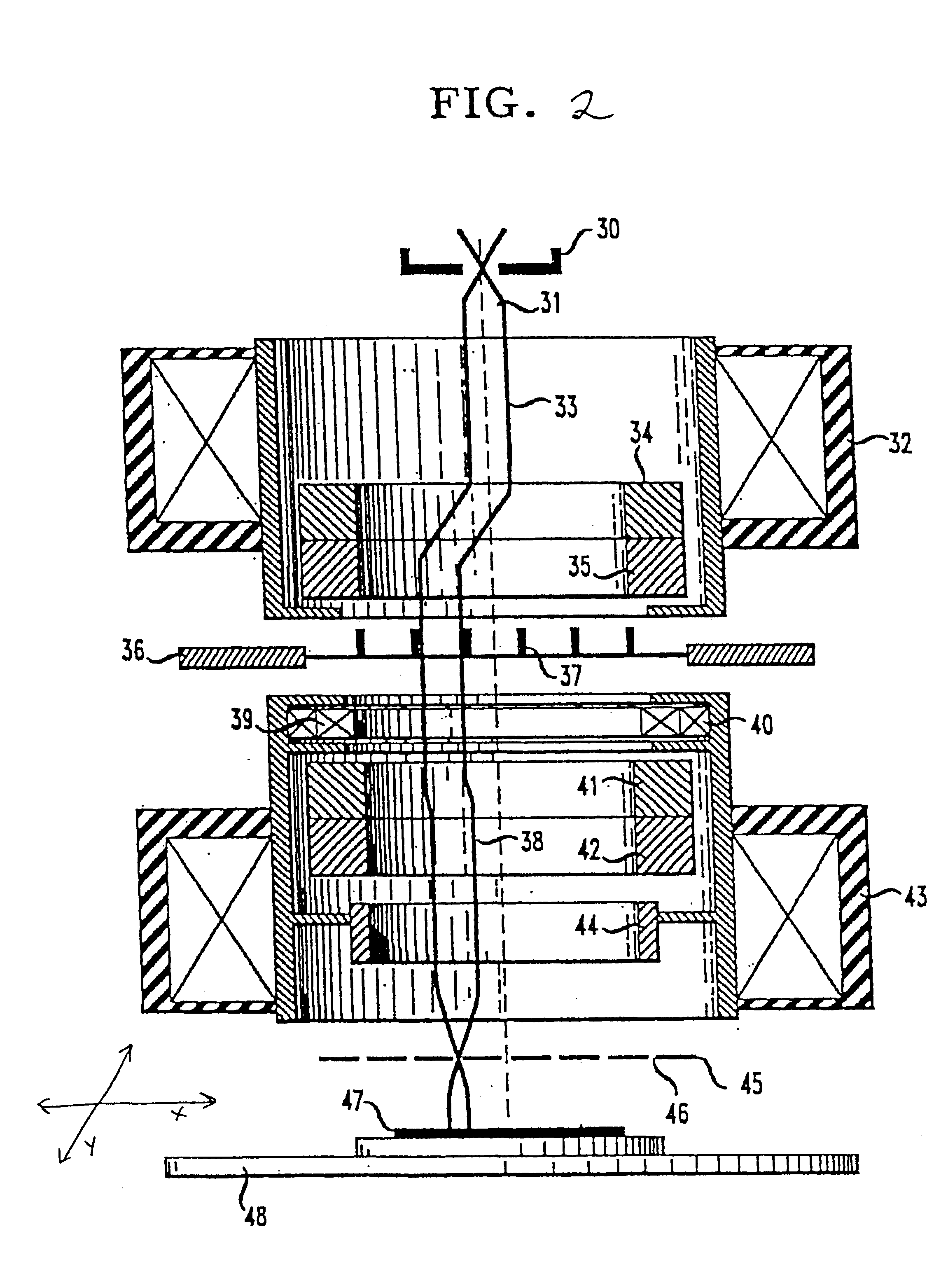
FIG. 11 illustrates an exemplary embodiment of an electron patterning system 100 of the present invention in one embodiment. The electron patterning system 100 may include a gun 102, a first lens system 104 (with an optical shaping aperture 106 at mid-plane), a blanking aperture 108, a second lens system 110, a mask 112, a projection doublet 114, including two lenses 116, 118 and a back focal plane 117 (with aperture 117a), and a wafer 120. FIG. 12 illustrates the mask 112, the projection doublet 114, and a wafer 120 in more detail. In particular, the lens 116 may include a magnetic shell 122, windings 124, and at least one deflector 126. An aperture 128 may be placed between the two lenses 116, 118. FIG. 12 also illustrates the relationship between the sub-field at the mask 112 and the sub-field at the wafer 120.
As discussed above with respect to FIG. 5, the goal is to place the wafer 120 of FIG. 11 in the plane where the image will be best focused. As outlined above, conventional ...
PUM
| Property | Measurement | Unit |
|---|---|---|
| angles | aaaaa | aaaaa |
| distance | aaaaa | aaaaa |
| energy | aaaaa | aaaaa |
Abstract
Description
Claims
Application Information


