Ultra thin body vertical replacement gate MOSFET

a technology of metal oxidesemiconductor and replacement gate, which is applied in the direction of basic electric elements, electrical equipment, and semiconductor devices, can solve the problems of reducing the scalability of electrostatic scalability in sub-35 nm devices, and affecting the scalability of electrostatic scalability

Inactive Publication Date: 2003-10-21
BELL SEMICON LLC
View PDF2 Cites 29 Cited by
  • Summary
  • Abstract
  • Description
  • Claims
  • Application Information

AI Technical Summary

Problems solved by technology

It is widely recognized that the two principal challenges to continued miniaturization of MOSFETs are electrostatic scalability and critical dimension control.
Since short-channel effects in PD-VRG MOSFETs are controlled by the doping level of the channel (known in the art as the body), it is difficult to provide electrostatic scalability in sub-35 nm devices; i.e., in devices in which the gate length is less than about 35 nm.
In addition, they can be fully depleted.

Method used


Image

  • Ultra thin body vertical replacement gate MOSFET
  • Ultra thin body vertical replacement gate MOSFET
  • Ultra thin body vertical replacement gate MOSFET

Examples


Embodiment Construction

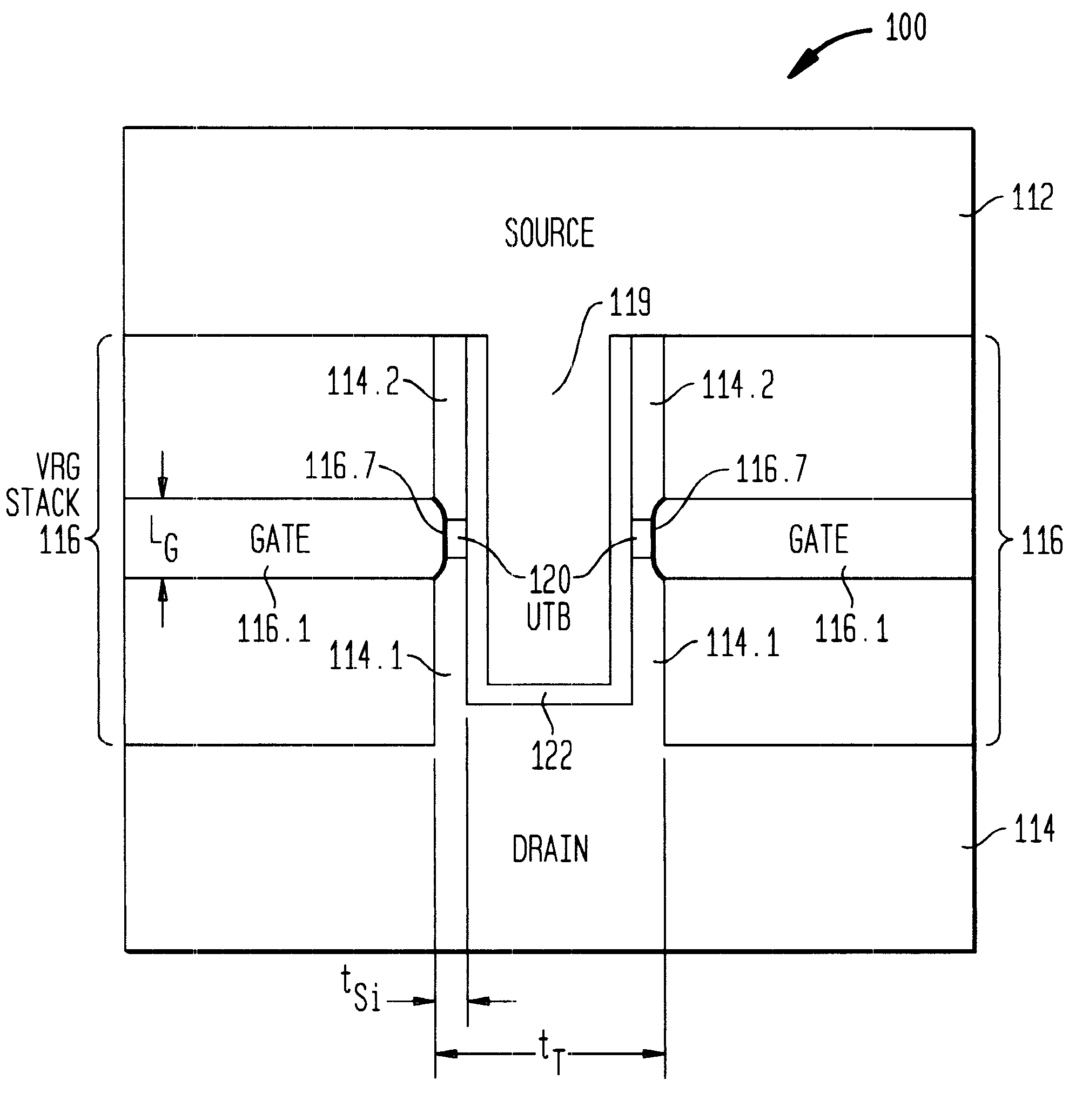
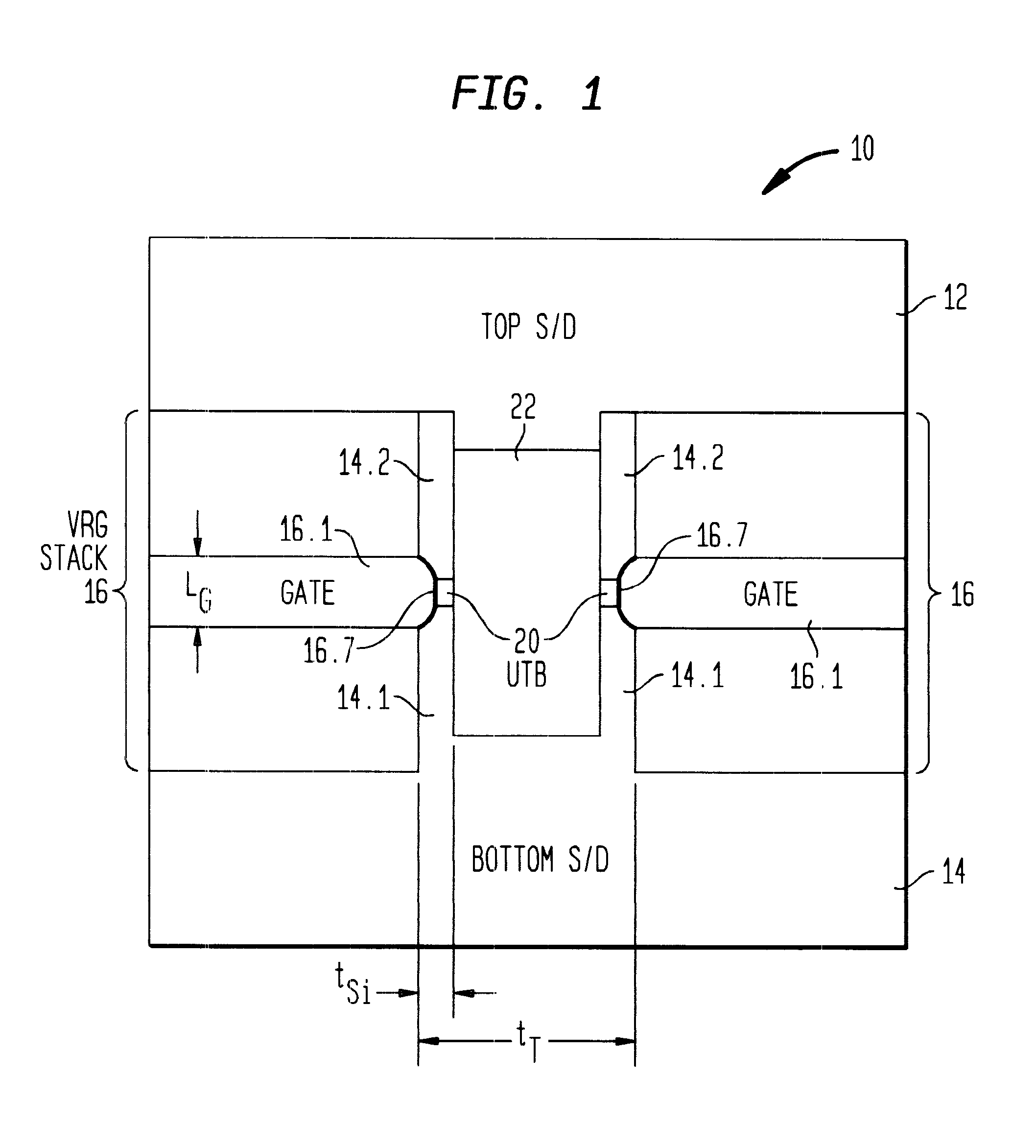
This example describes the fabrication a significant portion of an UTB-VRG-MOSFET of the type shown in FIG. 1, in accordance with one embodiment of our invention. Various materials, dimensions and operating conditions are provided by way of illustration only and, unless otherwise expressly stated, are not intended to limit the scope of the invention.

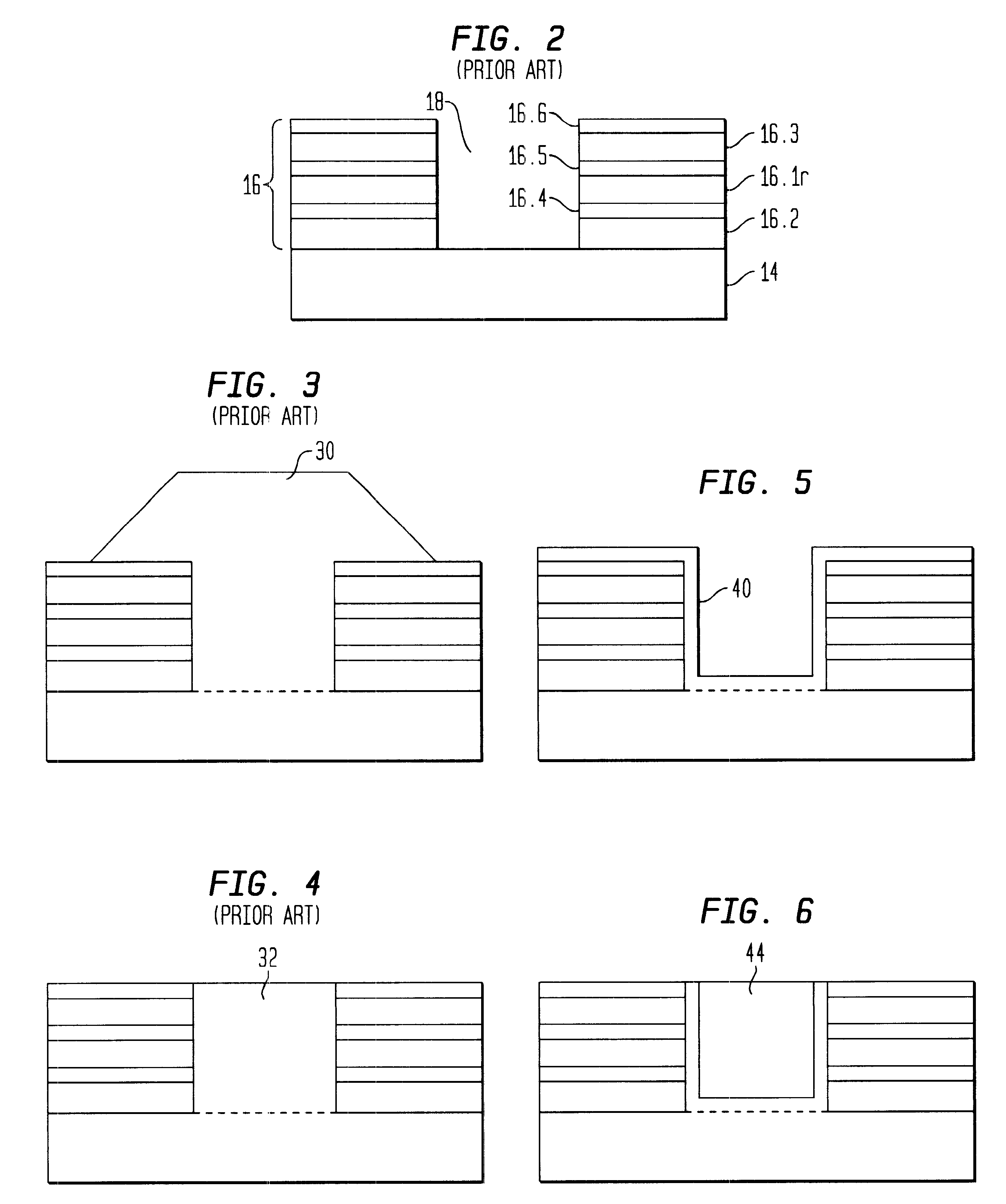
More specifically, the UTB-VRG-MOSFET of this example was fabricated by first forming a VRG stack and trench as depicted in FIG. 2. Then, in accordance with this example, an ultra thin (5-20 nm), undoped .alpha.-Si layer 40.1 (FIG. 7) was deposited in the trench and on a portion of the top surface of the stack. Next, a relatively thick (70 nm) sacrificial, doped x-Si layer 42.1 was deposited on the ultra thin layer 40.1 to facilitate recrystallization into x-Si. The sacrificial layer was doped with P to about 1-4.times.10.sup.20 cm.sup.-3. The stack was then annealed at 575.degree. C. in a nitrogen atmosphere for 2 hr. to recrystallize t...


PUM

PropertyMeasurementUnit
gate lengthaaaaaaaaaa
thickaaaaaaaaaa
total thicknessaaaaaaaaaa

Abstract

A method of fabricating a VRG MOSFET includes the steps of: (a) forming a VRG multilayer stack; (b) forming a trench in the stack; (c) depositing an ultra thin, amorphous semiconductor (alpha-semic) layer on the sidewalls of the trench (portions of the ultra thin layer on the sidewalls of the trench will ultimately form the channel or ultra thin body (UTB) of the MOSFET); (d) forming a thicker, alpha-semic sacrificial layer on the ultra thin layer; (e) annealing the alpha-semic layers to recrystallize them into single crystal layers; (f) selectively removing the recrystallized sacrificial layer; and (g) performing additional steps to complete the VRG MOSFET. In general, the sacrificial layer should facilitate the recrystallization of the ultra thin layer into single crystal material. In addition, the etch rate of the sacrificial layer should be sufficiently higher than that the ultra thin layer so that the sacrificial layer can be selectively removed in the presence of the ultra thin layer after recrystallization. The latter condition is illustratively satisfied by doping the sacrificial layer and by not (intentionally) doping the ultra thin layer. In accordance with one embodiment of our invention, step (g) includes filling the trench with oxide to form a thick back oxide region. In accordance with another embodiment of our invention, step (g) includes depositing a thin oxide layer (the back oxide) in the trench and then filling the remainder of the trench with a polycrystalline region (the back gate). VRG MOSFETs fabricated in accordance with our invention are expected to be electrostatically scalable with precise dimensional control. In addition, they can be fully depleted. Novel UTB device designs are also described.

Description

1. Field of the InventionThis invention relates to field effect transistors (FETs) and, more particularly, to metal-oxide-semiconductor (MOS) vertical FETs or vertical MOSFETs.2. Discussion of the Related ArtIt is widely recognized that the two principal challenges to continued miniaturization of MOSFETs are electrostatic scalability and critical dimension control. The vertical replacement gate (VRG) MOSFET provides precise control of all critical dimensions without lithography, while maintaining the essential features of advanced planar MOSFETs. The partially depleted (PD) VRG MOSFETs demonstrated to date are based on a thick, lithographically defined body. See, for example, J. M. Hergenrother et al., IEDM Tech. Dig., p. 75 (1999); S-H. Oh et al., IEDM Tech. Dig., p. 65 (2000); J. M. Hergenrother et al., IEDM Tech. Dig., p. 51 (2001); J. M. Hergenrother et al., Proc. 2.sup.nd European Workshop on the Ultimate Integration of Silicon (ULIS), p. 1 (2001); and J. M. Hergenrother et al....

Claims


Application Information

Patent Timeline
Patent Type & Authority Patents(United States)
IPC IPC(8): H01L21/70H01L21/8234
CPCH01L21/823487
Inventor HERGENROTHER, JOHN MICHAELKALAVADE, PRANAV
Owner BELL SEMICON LLC
Why Eureka
Try Eureka