Device manufacturing method

a manufacturing method and device technology, applied in the field of devices manufacturing methods, can solve the problems of pattern position distortion, pattern position distortion on the wafer, and limitation of resolution and position precision

Inactive Publication Date: 2003-11-11
CANON KK
View PDF7 Cites 1 Cited by
  • Summary
  • Abstract
  • Description
  • Claims
  • Application Information

AI Technical Summary

Benefits of technology

In the present invention, for dual or multiple exposures of different layers on a substrate, at least one pattern for each layer includes a portion having a common design rule. As a result of it, the pattern registration precision between different layers can be improved significantly. Thus, with the present invention, a pattern can be produced at higher resolution and precision, with a good registration precision between different layers.

Problems solved by technology

With this method, however, even if the exposure wavelength is shortened, there occurs an error (to be described later) which could not be disregarded in connection with the resolution and positional precision required, and it creates a limitation to the resolution and positional precisiion.
Further, depending on the flatness (irregularity) of a workpiece to be patterned, a pattern position distortion occurs.
In an exposure process using extreme ultraviolet rays, since the exposure process is performed by use of an original having been manufactured by use of an electron beam patterning apparatus such as described above, in addition to the positional distortion of the original itself, there occurs a pattern position distortion on a wafer due to aberrations produced in a projection optical system.
In an X-ray proximity exposure process, in addition to the positional distortion of an original itself produced by an electron beam patterning apparatus, there occurs a distortion of an X-ray mask.
Due to a stress distribution of the transmissive film or to a stress of the absorptive material, a positional distortion occurs.
Further, during the X-ray proximity exposure process, since the X-ray beam is not a completely parallel beam, there occurs a distortion, called a runout error.

Method used


Image

  • Device manufacturing method
  • Device manufacturing method
  • Device manufacturing method

Examples


example 2

A description will now be made of an example wherein a fine pattern is present at a central portion of first and second layers and wherein a large pattern is present in a peripheral portion of a picture angle of the second layer.

(First Layer Formation)

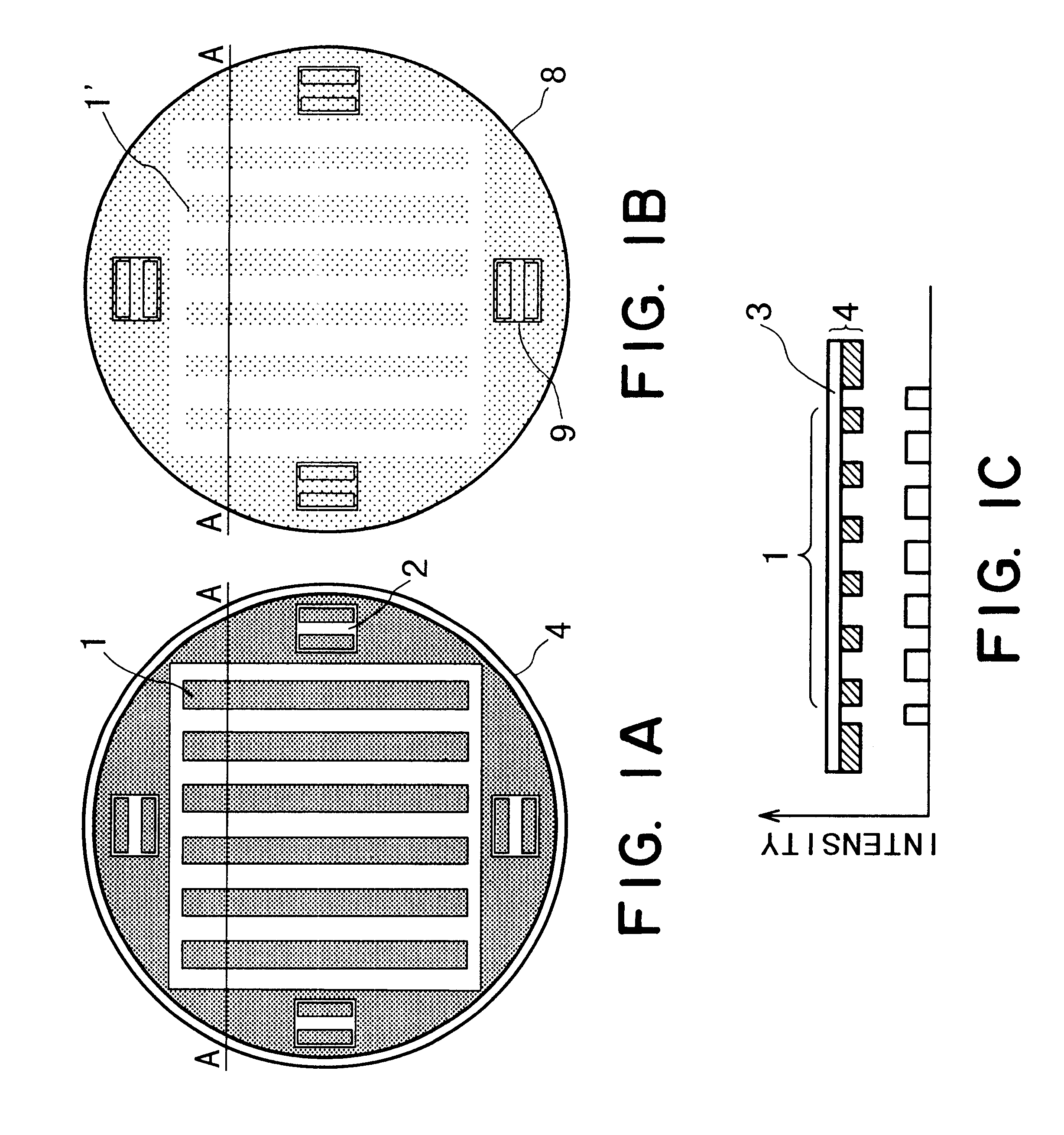
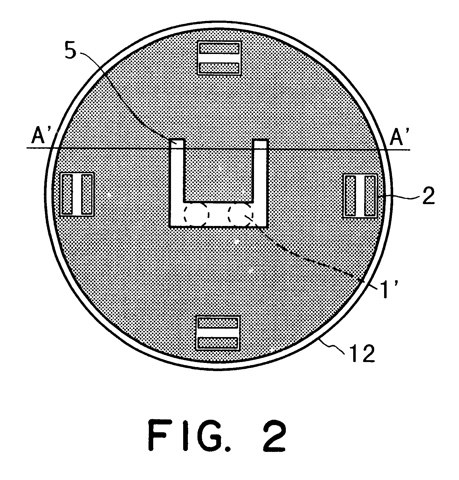
FIG. 9A shows a fine mask 4 (first mask) for a first layer, and it has a fine pattern 1 of periodic structure formed at a central portion (picture angle) of the mask. There are alignment marks 2 formed outside the picture angle. FIG. 9B shows a rough mask 12 (second mask) for the first layer, and it has a rough pattern 5 formed at a central portion (picture angle) of the mask. There are alignment marks 2 formed outside the picture angle.

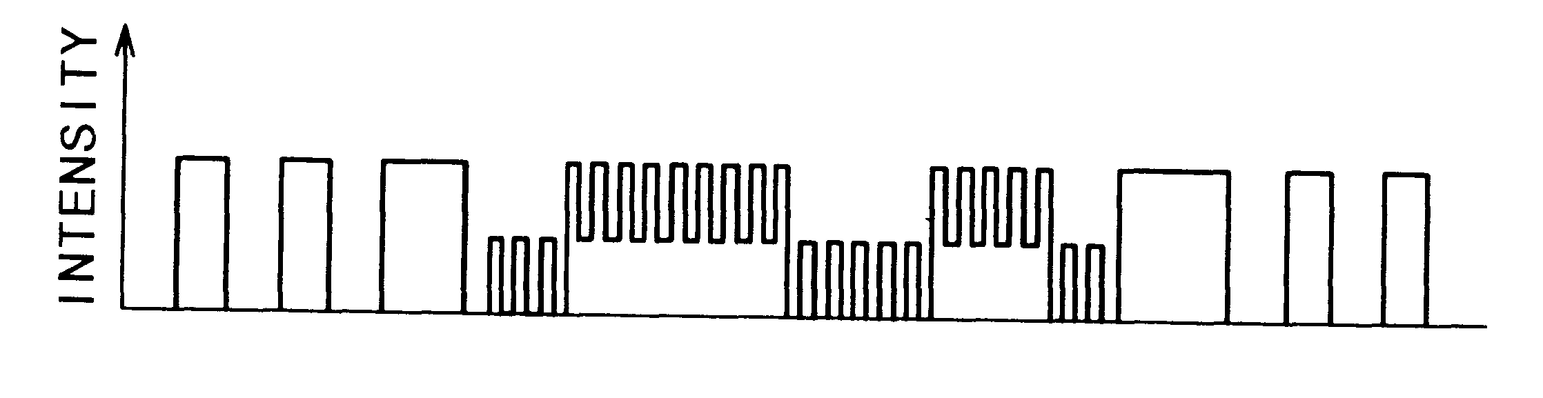
In this embodiment, an intensity distribution of a fine pattern image, of a period a half of the period of the fine pattern 1, is produced. This can be accomplished by controlling the spacing between the mask 1 and a wafer so that the same X-ray intensity is provided at the center of an absorptive mater...


PUM

PropertyMeasurementUnit
thicknessaaaaaaaaaa
thicknessaaaaaaaaaa
densityaaaaaaaaaa

Abstract

A device manufacturing method includes a first exposure step for executing a multiple exposure of a first layer of a substrate by use of plural first masks, a development step for developing the first layer of the substrate and a second exposure step, executed after the development step, for executing a multiple exposure of a second layer of the substrate by use of plural second masks. A portion of at least one of the first masks has a pattern the same as a pattern formed in a portion of at least one of the second masks.

Description

FIELD OF THE INVENTION AND RELATED ARTThis invention relates to a device manufacturing method usable for the manufacture of various electronic devices such as semiconductor chips (e.g., ICs or LSIs), display devices (e.g., magnetic heads) or image pickup devices (e.g., CCDs), for example.The density and speed of a semiconductor integrated circuit have been increased more and more, and the linewidth of an integrated circuit pattern has been narrowed more and more. This requires further improvements in semiconductor manufacturing methods. In some exposure apparatuses to be used for resist pattern formation in a lithographic process, among various semiconductor manufacturing processes, very short wavelengths of X-rays or extreme ultraviolet rays such as a KrF laser (248 nm), an ArF laser (193 nm), or an F.sub.2 laser (157 nm) are used.In an exposure process using extreme ultraviolet rays, mainly a reduction exposure of 1 / 4-1 / 5 is performed. A mask or reticle (original) is therefore for...

Claims


Application Information

Patent Timeline
Patent Type & Authority Patents(United States)
IPC IPC(8): G03F7/20H01L21/027
CPCG03F7/70466G03F7/2022H01L21/027
Inventor AMEMIYA, MITSUAKIUZAWA, SHUNICHICHIBA, KEIKOWATANABE, YUTAKA
Owner CANON KK
Why Eureka
Try Eureka