Method of forming mask pattern, method of forming thin film pattern and method of forming magnetoresistive element

a magnetoresistive element and mask pattern technology, applied in the field of mask pattern, can solve the problems of difficult removal of unnecessary seed layer, and achieve the effects of high structural stability, improved precision, and improved sensitivity

Active Publication Date: 2009-12-03
TDK CORPARATION
View PDF14 Cites 3 Cited by
  • Summary
  • Abstract
  • Description
  • Claims
  • Application Information

AI Technical Summary

Benefits of technology

[0013]In the method of forming a mask pattern according to an embodiment of the present invention, the inorganic film is formed so as to cover the upper surface of the photoresist pattern and the inside of the opening by a dry process, and the inorganic film on the upper surface of the photoresist pattern is removed by a dry etching process, then the photoresist pattern is removed, thereby the inorganic mask pattern corresponding to the opening has been obtained. In this manner, a mask pattern which is hardly deformed with high structural stability is available as compared with a mask pattern formed with a photoresist material, for example. In addition, steps of forming a seed layer and removing the seed layer are unnecessary, as compared with a mask pattern made of an inorganic material which is formed by frame plating process, for example. Accordingly, in the method of forming the first and second thin film patterns and the method of forming the MR element by use of the mask pattern according to an embodiment of the present invention, a fine thin film pattern can be formed more easily with higher resolution and precision.
[0014]In the method of forming a mask pattern according to an embodiment of the present invention, the photoresist pattern may be formed so that the opening may include a groove-shaped opening and a pair of other openings connected to both ends of the groove-shaped opening, respectively, the inorganic film may be formed by stacking a first inorganic layer and a second inorganic layer in order, and at least both ends, in the width direction, of a portion of the first inorganic layer included in the inorganic mas...

Problems solved by technology

In this case, it is difficult to remove the unnecessary seed layer w...

Method used


Image

  • Method of forming mask pattern, method of forming thin film pattern and method of forming magnetoresistive element
  • Method of forming mask pattern, method of forming thin film pattern and method of forming magnetoresistive element
  • Method of forming mask pattern, method of forming thin film pattern and method of forming magnetoresistive element

Examples


first embodiment

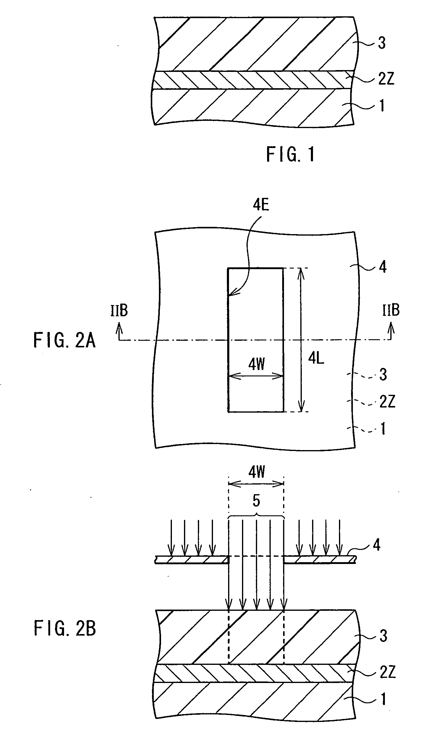
[0064]First, a method of forming a thin film pattern according to a first embodiment of the present invention will be described with reference to FIGS. 1 to 10. Here, a method of forming a mask pattern of the present invention will also be described together since it can be realized by the method of forming a thin film pattern, in which the mask pattern is used. The same is true for all the other embodiments.

[0065]The method of forming a thin film pattern of the present embodiment includes a step of forming a mask pattern, a first-half step of patterning to form a thin film pattern (a first thin film pattern), and a latter-half step of patterning to form another thin film pattern (second thin film pattern) disposed on both sides of the first thin film pattern, with the first thin film pattern in between. The step of forming a mask pattern includes steps of forming a photoresist pattern having an opening therein on a thin film to become the first thin film pattern, which is provided ...

second embodiment

[0080]Hereinbelow will be described the method of forming a thin film pattern as a second embodiment of the present invention with reference to FIGS. 11 to 20.

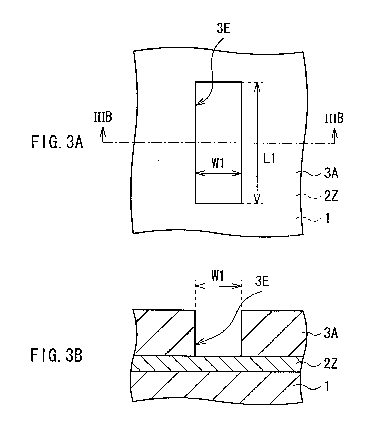
[0081]In the first embodiment, the inorganic film 7 is formed as one unit as shown in FIG. 5 using the photoresist pattern 3A with the groove-shaped opening 3E as shown in FIG. 3. Then, as shown in FIG. 7, the long and slender-shaped inorganic mask pattern 7Z is formed. On the other hand, in the present embodiment, a photoresist pattern is formed to have an opening configured of a groove-shaped opening and a pair of other openings connected to the both ends of the groove-shaped opening, and an inorganic film is formed by stacking a first inorganic layer and a second inorganic layer in order, then the photoresist pattern is removed, thereby obtaining an inorganic mask pattern. After this, a portion of the first inorganic layer included in the inorganic mask pattern, corresponding to the groove-shaped opening, is dissolved and r...

third embodiment

[0095]Subsequently, a method of forming a thin film pattern according to a third embodiment of the present invention will be described hereinbelow with reference to FIGS. 22 to 31.

[0096]In the first embodiment, the inorganic film 7 is formed as one unit as shown in FIG. 5 using the photoresist pattern 3A with the groove-shaped opening 3E provided on the thin film 2Z as shown in FIG. 3. Then, as shown in FIG. 7, the long and slender inorganic mask pattern 7Z is formed. In the second embodiment, the photoresist pattern 9A is formed to have the pair of other openings 9E2 connected to the both ends of the groove-shaped opening 9E1 on the thin film 2Z as shown in FIG. 12, the inorganic film is formed by stacking the inorganic layer 10 and the inorganic layer 11 in order as shown in FIGS. 13 and 14, then the photoresist pattern 9A is removed, thereby obtaining the inorganic mask pattern 11Y. After this, as shown in FIG. 17, the area 10A, which is included in the inorganic layer 10 constit...


PUM

PropertyMeasurementUnit
Widthaaaaaaaaaa
Dimensionaaaaaaaaaa
Magnetismaaaaaaaaaa

Abstract

In the present invention, provided is a method of forming a mask pattern by which a fine thin film pattern may be formed more easily with higher resolution and precision. In the method of forming a mask pattern, a photoresist pattern having an opening is formed on a substrate, then, an inorganic film is formed so as to cover the upper surface of the photoresist pattern and the inside of the opening, then the inorganic film on the upper surface of the photoresist pattern is removed by a dry etching process. Subsequently, an inorganic mask pattern is formed by removing the photoresist pattern. The inorganic mask pattern thus formed hardly produces an issue of deformation such as physical displacement even when it is heated in the dry etching process.

Description

BACKGROUND OF THE INVENTION[0001]1. Field of the Invention[0002]The present invention relates to a method of forming a mask pattern suitable for forming a fine thin film pattern, a method of forming a thin film pattern and a method of forming an MR element using the mask pattern.[0003]2. Description of the Related Art[0004]Conventionally, various thin film patterns are used in many ways in the electronic and magnetic devices such as a thin film magnetic head and a semiconductor device formed through a thin-film formation process. Generally, a dry etching process is used to form such thin film patterns, and a mask pattern is necessary in this process. Here, a thin film is formed at first to cover the whole surface of a substrate, then a photoresist pattern with a desired pattern shape is formed on the thin film by photolithography, etc. Subsequently, a dry etching process such as ion milling is applied to the thin film using the photoresist pattern as a mask, thereby a thin film patt...

Claims


Application Information

Patent Timeline
IPC IPC(8): B44C1/22C23F1/00
CPCB82Y10/00B82Y25/00G11B2005/3996G11B5/3909G11B5/3932G01R33/098
Inventor KAMIJIMA, AKIFUMIYATSU, HIDEYUKIHATATE, HITOSHI
Owner TDK CORPARATION
Why Eureka
Try Eureka