Alternating current driven type plasma display device and method for production thereof

a technology of alternating current and display device, which is applied in static indicating devices, instruments, gas-filled discharge tubes, etc., can solve the problems of low brightness of glow discharge and inability to easily take place in the space above the discharge gap, so as to increase the amount of charge accumulation and improve the brightness

Inactive Publication Date: 2003-12-02
SONY CORP
View PDF10 Cites 26 Cited by
  • Summary
  • Abstract
  • Description
  • Claims
  • Application Information

AI Technical Summary

Benefits of technology

It is therefore a first object of the present invention to provide an alternating current driven type plasma display device structured to increase a charge accumulation amount for improving the brightness, and a method for the production thereof.
When the distance between the electrodes comes to be less than 5.times.10.sup.-5 m, presumably, the cathode glow B is positioned in the central area between the electrodes and the Aston dark spaces A appear on both sides of the cathode glow B as is schematically shown in FIG. 22B. In some cases, the negative glow can partly exist. In the tri-electrode type plasma display device, the cathode glow is formed in a space region near a surface portion of the dielectric material layer which portion covers one sustain electrode corresponding to the cathode or a space region near a surface portion of the dielectric material layer which portion covers the other sustain electrode corresponding to the cathode. When the distance between a pair of the sustain electrodes is arranged to be less than 5.times.10.sup.-5 m as described above, and when the pressure in the space is adjusted to 1.0.times.10.sup.2 Pa (0.001 atmospheric pressure) to 3.0.times.10.sup.5 Pa (3 atmospheric pressures), the cathode glow can be used as a discharge mode. A high AC glow discharge efficiency can be therefore achieved, and as a result, a high light-emission efficiency and high brightness can be attained in the plasma display device.

Problems solved by technology

The problem with presently commercialized AC plasma display devices is that that the brightness thereof is low.
That is, when the dielectric material layer 14 has a large thickness relative to the discharge gap, most electric lines of flux pass through the dielectric material layer 14, and as a result, glow discharge does not easily take place in the space above the discharge gap.

Method used


Image

  • Alternating current driven type plasma display device and method for production thereof
  • Alternating current driven type plasma display device and method for production thereof
  • Alternating current driven type plasma display device and method for production thereof

Examples


example 1

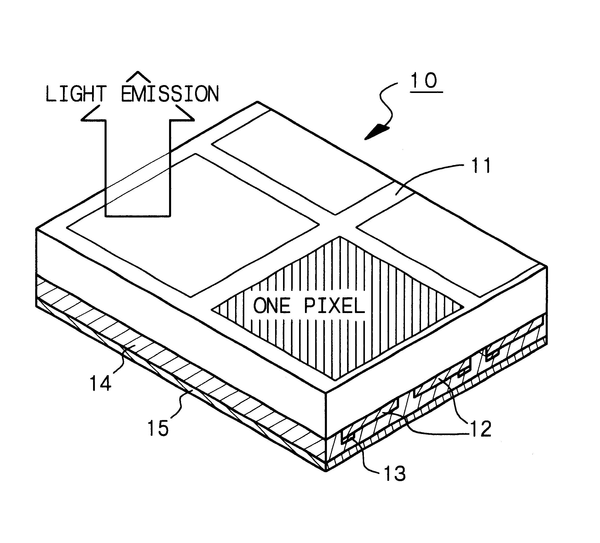
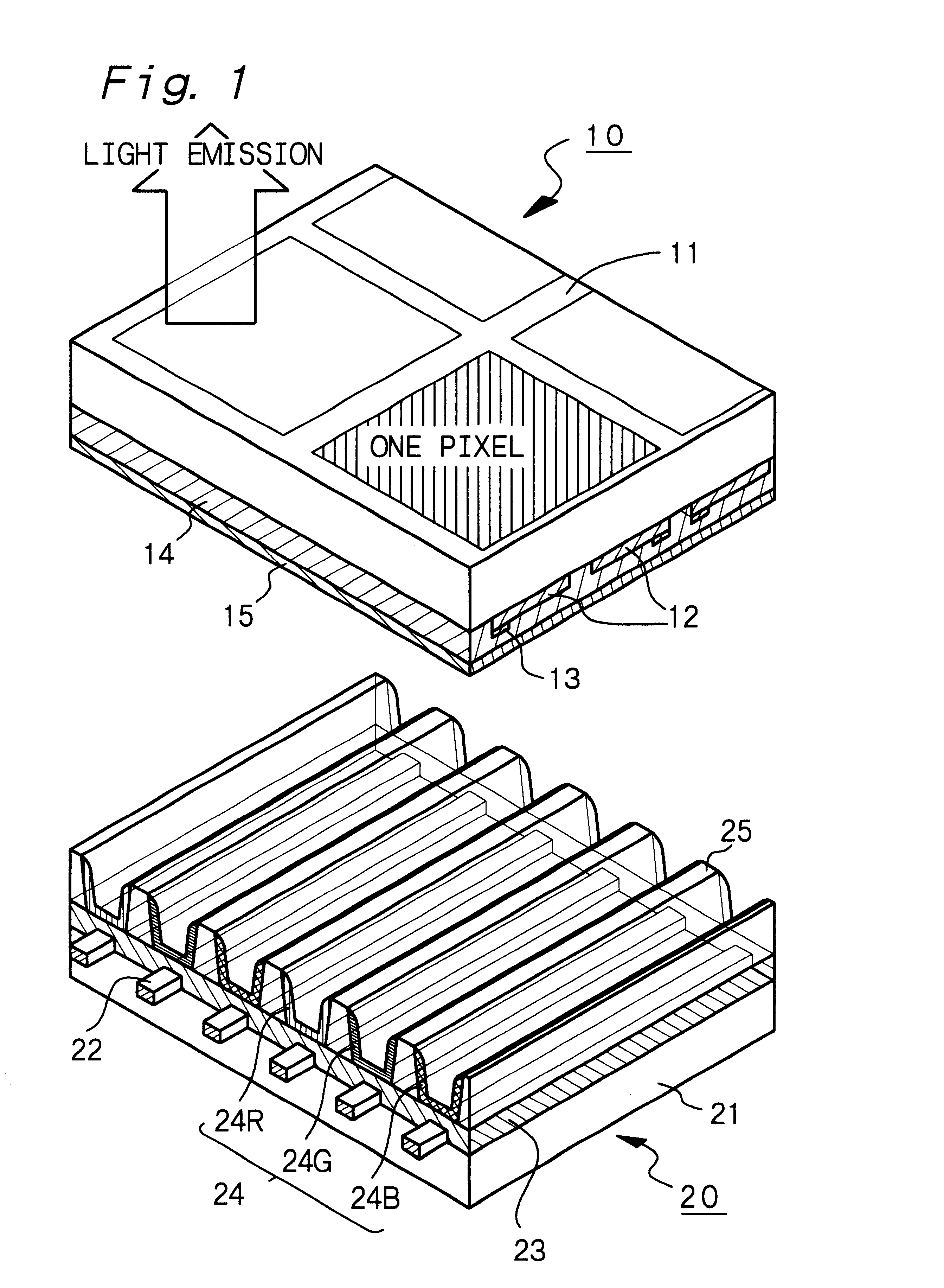
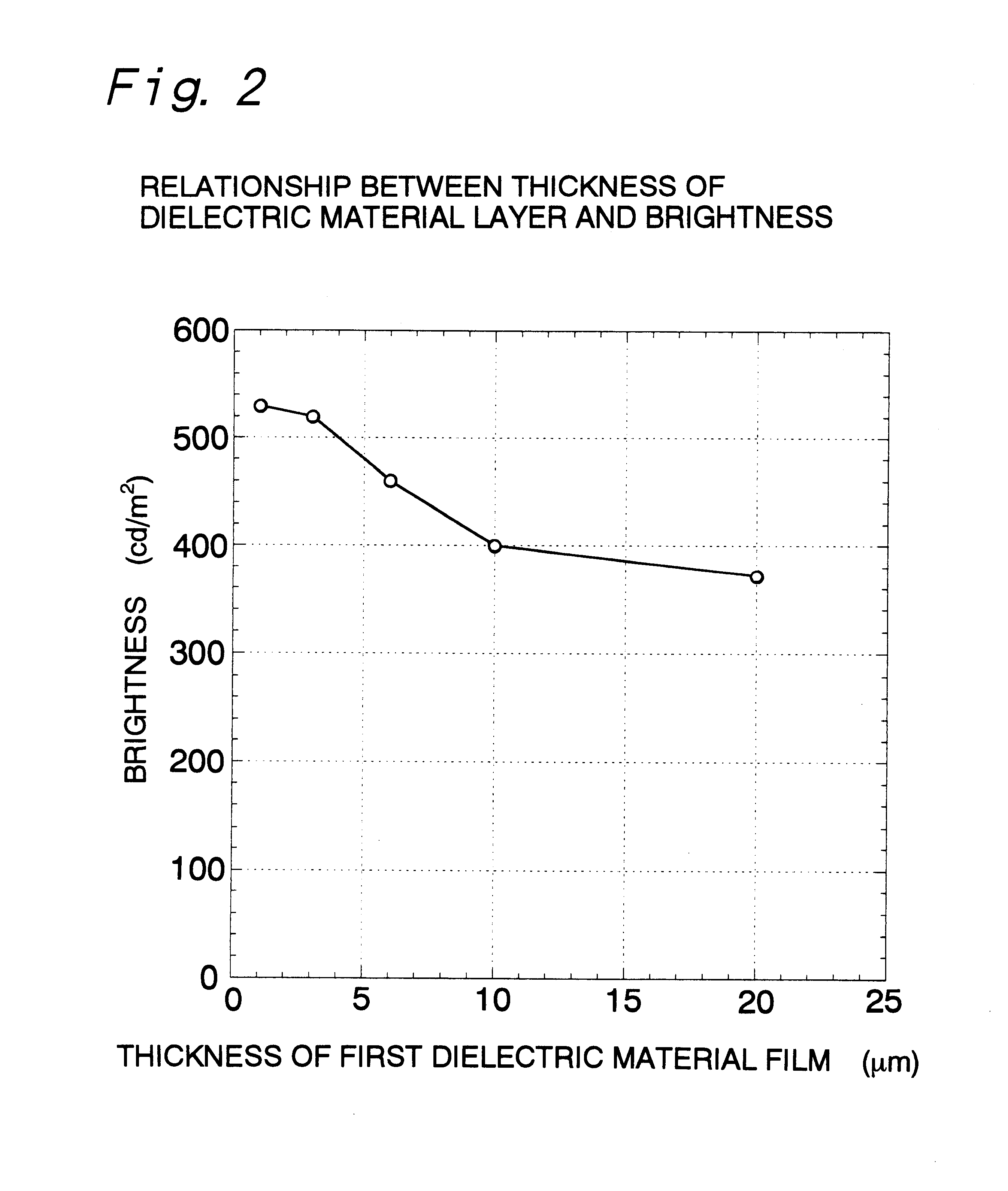
is concerned with the alternating current driven type plasma display devices (to be referred to as "plasma display device" hereinafter) according to the first and fourth aspects of the present invention. The plasma display device of Example 1 has a characteristic feature in that a dielectric material layer has a thickness of 1.5.times.10.sup.-5 m or less. The dielectric material layer comprised a first dielectric material film composed of silicon oxide (SiO.sub.x) and a second dielectric material film composed of MgO and formed thereon. A tri-electrode type plasma display device according to the first aspect of the present invention, having a structure shown in FIG. 1, was produced by a method to be explained below.

The first panel 10 was produced by the following method. First, an ITO layer was formed on the entire surface of the first substrate 11 composed of high-distortion-point glass or soda glass by a sputtering method, and the ITO layer was patterned in the form of stripes by ...

example 2

Example 2 is also concerned with the plasma display devices according to the first and fourth aspects of the present invention. In Example 2, the distance between a pair of the sustain electrodes 12 was varied, and a relationship between the brightness of a thus-obtained plasma display device and the distance between a pair of the sustain electrodes 12 was studied. In Example 2 or Examples 3 to 7, tri-electrode type plasma display devices structured as shown in FIG. 1 were produced.

In Example 2, the first panel 10 was produced by the following method. First, procedures up to the formation of the bus electrode 13 were carried out in the same manner as in Example 1. Then, a 3 .mu.m thick first dielectric material film 14 composed of silicon oxide was formed on the entire surface in the same manner as in Example 1. Otherwise, a 10 .mu.m thick first dielectric material film 14 composed of silicon oxide was formed on the entire surface by a screen printing method. Then, a 0.6 .mu.m thick...

example 3

Example 3 is concerned with the plasma display device according to the second aspect of the present invention. In the plasma display device of Example 3, the dielectric material layer comprised a first dielectric material film constituted of an aluminum oxide layer and a second dielectric material film composed of MgO and formed thereon.

The first panel was produced by the following method. First, procedures up to the formation of the bus electrode 13 were carried out in the same manner as in Example 1. Then, the first dielectric material film 14 composed of aluminum oxide was formed by an electron beam heating method under a condition shown in Table 2 below. In this case, the first dielectric material film 14 had a thickness of 1 .mu.m to 20 .mu.m. Then, a 0.6 .mu.m thick second dielectric material film (protective film) 15 composed of magnesium oxide (MgO) was formed on the first dielectric material film 14 by an electron beam deposition method. By the above steps, the first panel ...


PUM


Abstract

An alternating current driven type plasma display device comprising a first panel and a second panel, said first panel having sustain electrodes formed on a first substrate and a dielectric material layer formed on the first substrate and the sustain electrodes, wherein the first panel and the second panel are bonded to each other in their circumferential portions,characterized in that the dielectric material layer has a thickness of 1.5x10<-5 >m or less.

Description

BACKGROUND OF THE INVENTION AND RELATED ART STATEMENTThe present invention relates to an alternating current driven type plasma display device having a characteristic feature in a dielectric material layer and a method for the production thereof.As an image display device that can be substituted for a currently mainstream cathode ray tube (CRT), flat-screen (flat-panel) display devices are studied in various ways. Such fat-panel display devices include a liquid crystal display (LCD), an electroluminescence display (ELD) and a plasma display device (PDP). Of these, the plasma display device has advantages that it is relatively easy to form a larger screen and attain a wider viewing angle, that it has excellent durability against environmental factors such as temperatures, magnetism, vibrations, etc., and that it has a long lifetime. The plasma display device is therefore expected to be applicable not only to a home-use wall-hung television set but also to a large-sized public informa...

Claims


Application Information

Patent Timeline
Patent Type & Authority Patents(United States)
IPC IPC(8): H01J17/49
CPCH01J11/12H01J11/24H01J11/38H01J2211/323H01J2211/245
Inventor NAKADA, SATOSHIUTSUMI, ICHIROMORI, HIROSHIYOSHIKAWA, EITAROKIMURA, TOMOHIROONIKI, KAZUNAOSHIROZU, SHINICHIRO
Owner SONY CORP
Why Eureka
Try Eureka