Electro-optic device and electronic apparatus

a technology of optical devices and electronic devices, applied in the field of optical devices, can solve the problems of increased size of electro-optic devices, waste of space, and higher probability of short-circuiting between both substrates, so as to reduce distance, prevent short-circuiting, and ensure reliability in the electrical conduction region between both substrates.

Inactive Publication Date: 2003-12-16
BOE TECH GRP CO LTD
View PDF10 Cites 26 Cited by
  • Summary
  • Abstract
  • Description
  • Claims
  • Application Information

AI Technical Summary

Benefits of technology

In the electro-optic device of the present invention, the first electrode extending simply in the direction of length from one side of the first substrate, on which the driving IC is mounted, toward the other opposing side thereof is connected through electrical conduction between the first substrate and the second substrate. To the second electrode which is routed toward the outer side to bypass the first electrode and is extended in the direction of width, a signal is directly supplied from the driving IC through the same substrate as that on which the driving IC is mounted. Therefore, there is no need of utilizing the electrical conduction between both the substrates in a region where patterns must be obliquely extended. Thus, in the region where patterns must be obliquely extended, it is only necessary to form the second electrode which can be formed with a reduced distance between the patterns. Accordingly, the necessity of reducing the spacing between the intersubstrate conducting terminal portions is eliminated even when the number of patterns is increased in the region where the patterns must be obliquely extended. With the present invention, therefore, reliability in the region of the electrical conduction between both the substrates does not deteriorate even in cases where the number of electrodes is increased.
Also, the second electrode, which is subjected to such a restriction on electrode layout that patterns must be obliquely extended, is formed of, e.g., a metallic film having smaller electrical resistance than an ITO film. With this feature, electrical characteristics are kept from deteriorating regardless of a reduction in the line width of the wiring portion of the second electrode, which does not take part in constituting pixels. Accordingly, the present invention can prevent display quality from degrading due to deterioration of the electrical characteristics even when the number of electrodes is increased. Conversely speaking, given the number of patterns being the same, the region of the second substrate, in which patterns must be obliquely extended, can be made narrower than required in the conventional construction. In the electro-optic device having the same outer dimensions, it is possible to enlarge an image display area. Further, since the region of the second substrate, in which patterns must be obliquely extended, can be made narrower than required in the conventional construction, it is possible to reduce the outer dimensions of the electro-optic device having an image display area that is the same size as in conventional devices. Additionally, the electro-optic device utilizing the COG mounting technique is more inexpensive than another one utilizing the COF or TAB mounting technique, and has higher reliability in resistance to peeling-off because it includes no connection to a flexible board such as a thin film or TAB carrier.

Problems solved by technology

However, such a construction has the problem that the size of the electro-optic device is increased because the first transparent substrate 10Z and the second transparent substrate 20Z have the extended portions 25', 25".
However, since the electrical conduction between both the substrates is conventionally established using the inter-substrate conducting terminal portions 70Y having the obliquely extending zones, there arises a problem that a sufficient spacing between the inclined zones 702Y of the adjacent terminal portions 70Y must be ensured by forming the straight zones 701Y to have lengths differing from each other to a relatively large extent, thus resulting in wasteful use of an area that is positioned outside the image display area 2 and includes the inter-substrate conducting terminal portions 70Y.
This results in a higher probability that a short-circuiting may occur between both the substrates.

Method used


Image

  • Electro-optic device and electronic apparatus
  • Electro-optic device and electronic apparatus
  • Electro-optic device and electronic apparatus

Examples


embodiment 1

On the first transparent substrate 10, as with Embodiment 1 described above by referring to FIG. 3, sets of color filters 7R, 7G and 7B of red (R), green (G) and blue (B) are formed in areas corresponding to points at which the first electrodes 40 intersect the second electrodes 50. An insulating flattening film 11, the first electrodes 40 and an alignment film 12 are formed in this order on the surface side of the color filters 7R, 7G and 7B. On the second transparent substrate 20, the second electrodes 50 and an alignment film 22 are formed in this order.

In the electro-optic device 1, the first electrodes 40 are formed of an ITO film (transparent conductive film). On the other hand, the second electrodes 50 are formed of a metallic film (conductive film) capable of reflecting light, such as an aluminum film, an alloy film made of primarily aluminum, a silver film, or a silver alloy film made of primarily silver.

Also, in the electro-optic device 1 of this embodiment, as shown in FI...

embodiment 2

In Embodiment 2 described above, the second electrodes 50 comprises the drive portions 51 extending straight over the image display area 2, and the wiring portions 52 routed from the drive portions 51 up to the area in which the driving IC 7 is mounted, the wiring portions 52 being formed on both outer sides of the first terminals 81 in the direction of width of the second transparent substrate 20. However, the terminal arrangement may be modified such that the second electrodes 50 may be routed from the area, in which the driving IC 7 is mounted, to pass through only one side outward of the first terminals 81 in the direction of width of the second transparent substrate 20, and may be then extended from that one side to the image display area 2.

embodiment 3

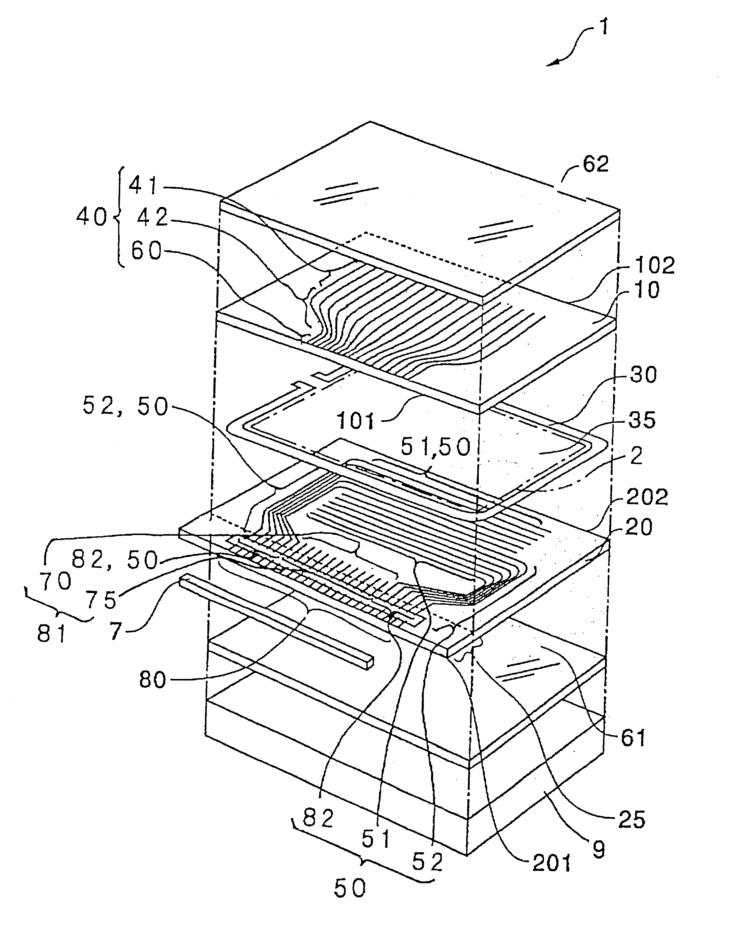
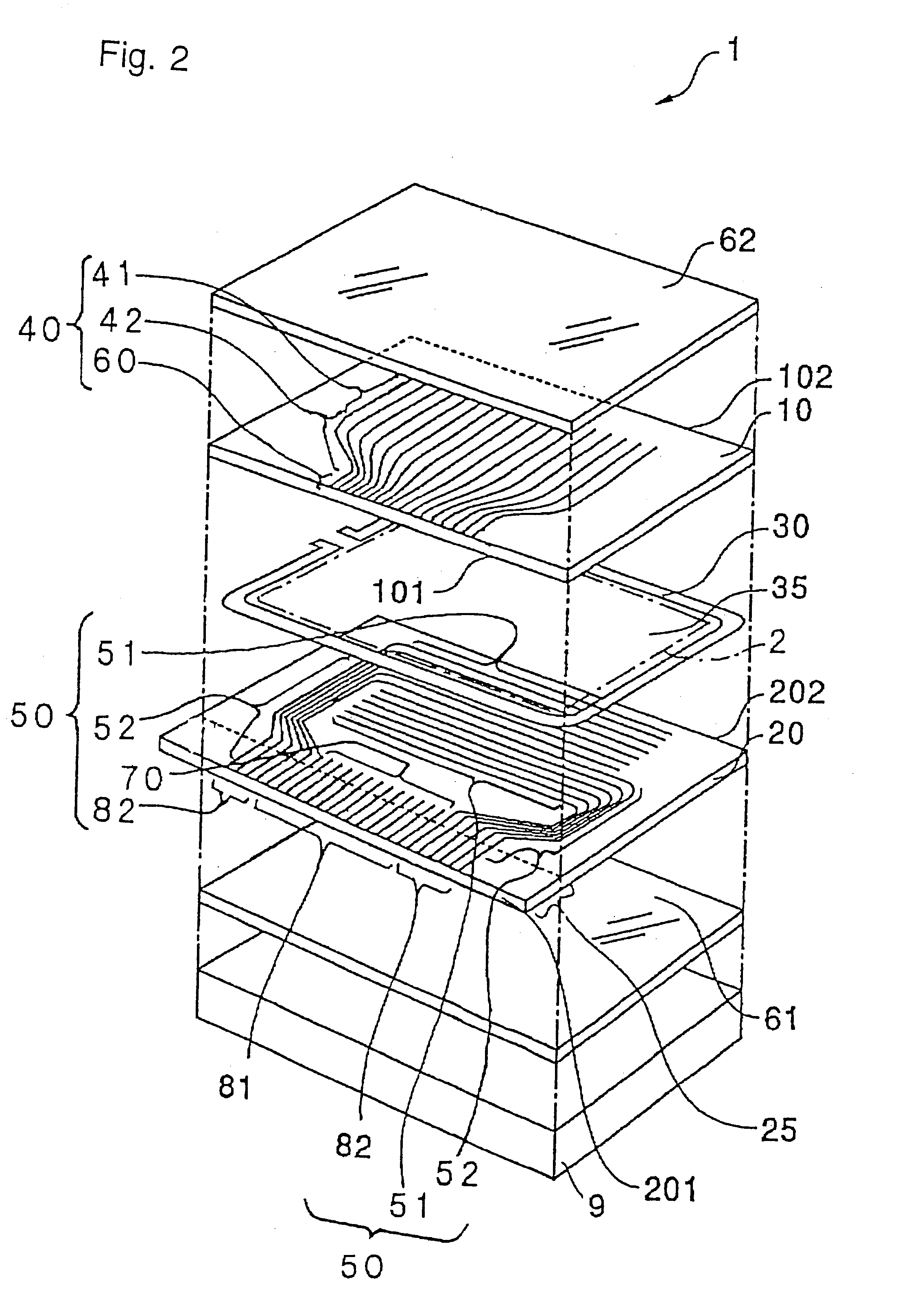
FIGS. 13 and 14 are respectively a perspective view showing the construction of an electro-optic device 1 of the present invention, and an exploded perspective view of the electro-optic device 1.

As shown in FIGS. 13 and 14, the electro-optic device 1 of this embodiment comprises a first transparent substrate 10 and a second transparent substrate 20 arranged in an opposed relation, a sealing member 30 applied in the form of a rectangular frame for bonding both the substrates to each other, and a liquid crystal layer 4 sealed in a liquid crystal sealed-in space 35 surrounded by the first transparent substrate 10, the second transparent substrate 20, and the sealing member 30. Of the liquid crystal sealed-in space 35, an area in which later-described pixels are arrayed in a matrix pattern serves as an image display area 2.

The first transparent substrate 10 and the second transparent substrate 20 are each a plate-like member made of quartz, glass, plastic or the like. A plurality of el...


PUM

PropertyMeasurementUnit
electric fieldaaaaaaaaaa
electrical resistanceaaaaaaaaaa
electrically conductingaaaaaaaaaa

Abstract

In an electro-optic device 1, connection to first electrodes 40 of a first transparent substrate 10 extending in one direction from the side, to which signals are inputted, is established through electrical conduction between two substrates in a width-wise central area of the first transparent substrate using first terminals 81. To second electrodes 50 of a second transparent substrate 20 which are routed toward the outer side, signals are directly inputted from second terminals 82. The obliquely routed second electrodes 50 are formed of, e.g., an aluminum alloy film, and slit-like openings are formed in the second electrodes 50 to allow passage of light emitted from a backlight device 9.

Description

BACKGROUND OF THE INVENTION1. Technical Field of the InventionThe present invention relates to an electro-optic device having an electro-optic substance held between a pair of substrates, and an electronic apparatus employing the electro-optic device. More specifically, the present invention relates to the structure of electrodes and terminals in each of the substrates constituting the electro-optic device.2. Description of the Related ArtOf various types of electro-optic devices, one (liquid crystal device) utilizing a liquid crystal as an electro-optic substance comprises, as shown in FIG. 21, a first transparent substrate 10Z and a second transparent substrate 20Z arranged in an opposed relation, a sealing material 30 for bonding both the substrates to each other, and a liquid crystal sealed in an area surrounded by the first transparent substrate 10Z, the second transparent substrate 20Z and the sealing material 30. In a state of the first transparent substrate 10Z and the secon...

Claims


Application Information

Patent Timeline
Patent Type & Authority Patents(United States)
IPC IPC(8): G02F1/13G02F1/1345G02F1/1343G09F9/30G09F9/35
CPCG02F1/1345G02F2001/133342G02F1/13452G02F1/133342G02F1/1343
Inventor HAGIWARA, TAKESHI
Owner BOE TECH GRP CO LTD
Why Eureka
Try Eureka