Non-contact IC card and IC card communication system

a communication system and non-contact technology, applied in the field of non-contact ic cards, can solve the problems of difficult to maintain a high mechanical strength of such a card, the inability to control the distance between the substrate and the ic chip using the au bump, etc., and achieve the effect of maintaining communication characteristics, enhancing the connection reliability of the mounting portion of the ic chip, and high mechanical strength

Inactive Publication Date: 2003-12-23
KK TOSHIBA
View PDF10 Cites 45 Cited by
  • Summary
  • Abstract
  • Description
  • Claims
  • Application Information

AI Technical Summary

Benefits of technology

It is therefore an object of the present invention to eliminate the aforementioned problems and to provide a non-contact IC card capable of enhancing the connection reliability of an IC chip mounting portion, maintaining communication characteristics, and maintaining a high mechanical strength, and a communication system using the same.
In order to accomplish the aforementioned and other objects, according to one aspect of the present invention, a non-contact IC card comprises: a substantially rectangular insulating substrate; a semiconductor chip mounted on a first face of the insulating substrate; and an antenna coil for transmitting information and for enhancing the mechanical strength of the insulating substrate, the antenna coil being arranged on the first face of the insulating substrate along the outer periphery of the first face, and the antenna coil having first and second connecting terminals which are connected to the semiconductor chip.
According to another aspect of the present invention, an IC card communication system comprises a non-contact IC card and a reader / writer, the non-contact IC card comprising: a substantially rectangular insulating substrate; a semiconductor chip mounted on a first face of the insulating substrate; and an antenna coil for transmitting information and for enhancing the mechanical strength of the insulating substrate, the antenna coil being arranged on the first face of the insulating substrate along the outer periphery of the first face, and the antenna coil having first and second connecting terminals which are connected to the semiconductor chip, and the non-contact IC card transmitting signals from and to the reader / writer via the antenna coil by the electromagnetic induction.

Problems solved by technology

However, if the conductor is made of a soft material, such as Al foil or Ag paste, the bump is embedded into the conductor, so that the distance between the substrate and the IC chip can not be controlled by using the Au bump.
However, in general, it is very difficult for such a card to maintain a high mechanical strength.

Method used


Image

  • Non-contact IC card and IC card communication system
  • Non-contact IC card and IC card communication system
  • Non-contact IC card and IC card communication system

Examples


Embodiment Construction

Referring now to the accompanying drawings, the preferred embodiments of the present invention will be described below.

First, referring to FIGS. 1, 2, 7 and 8, the first preferred embodiment of the present invention will be described.

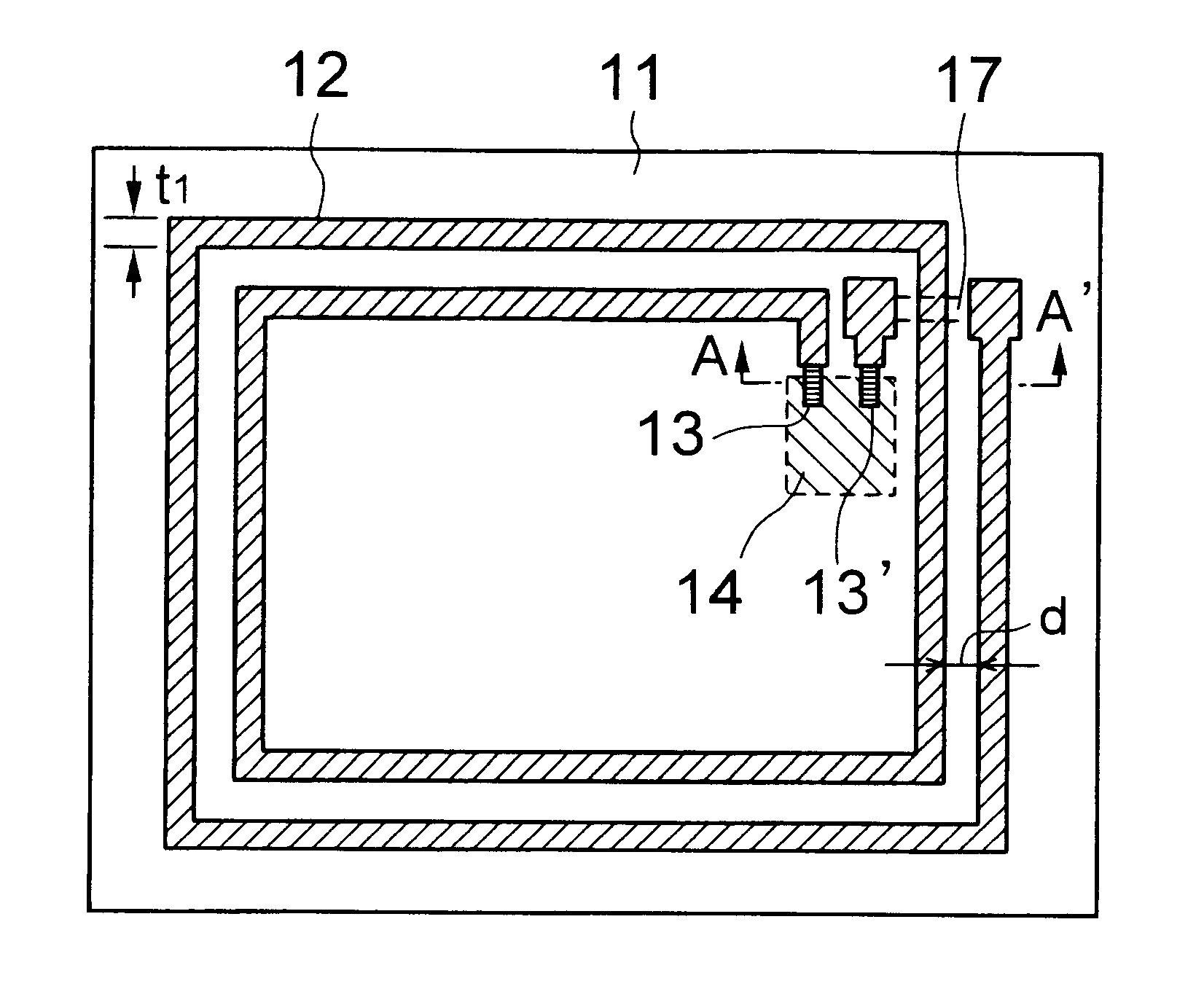
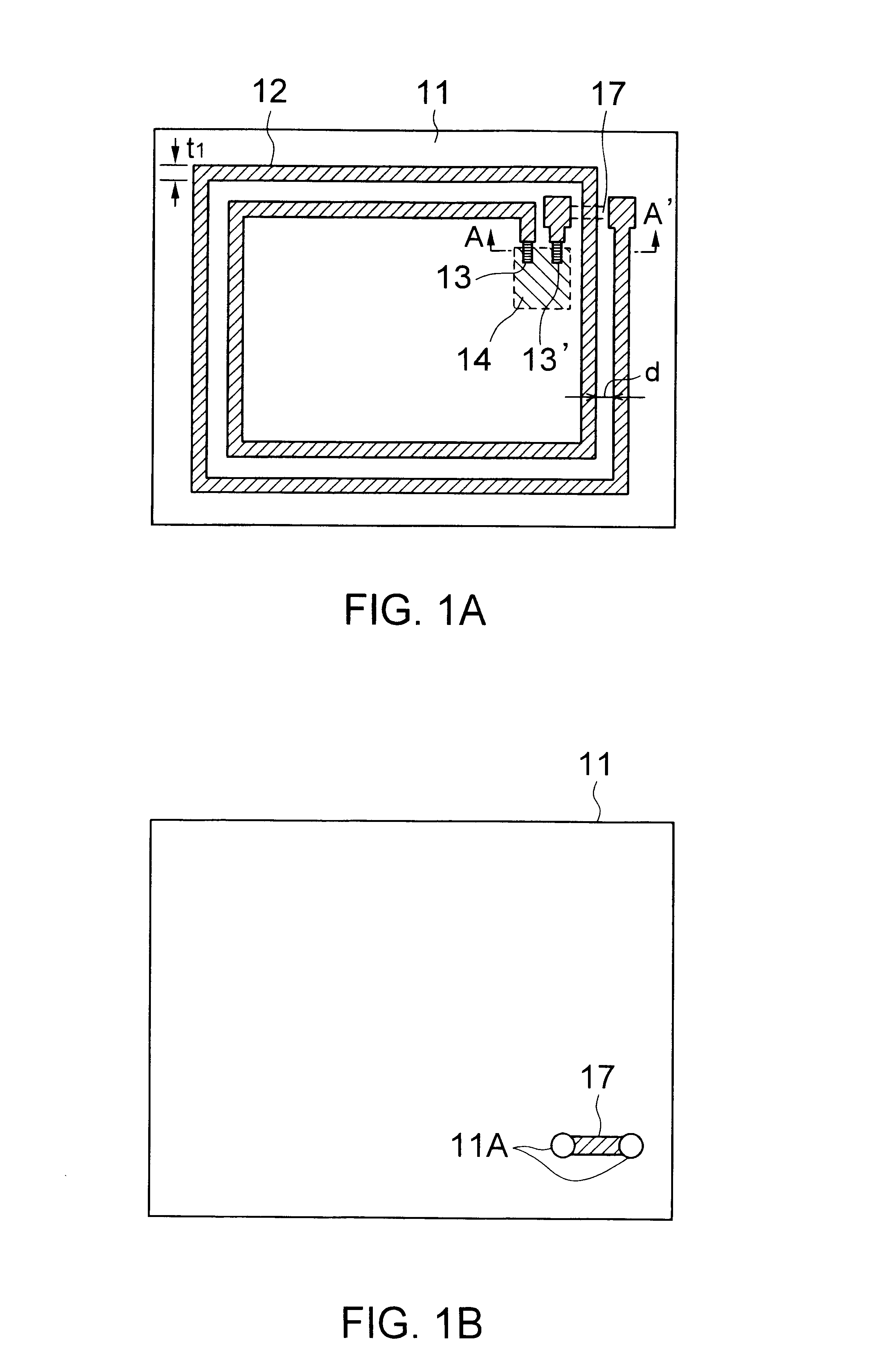
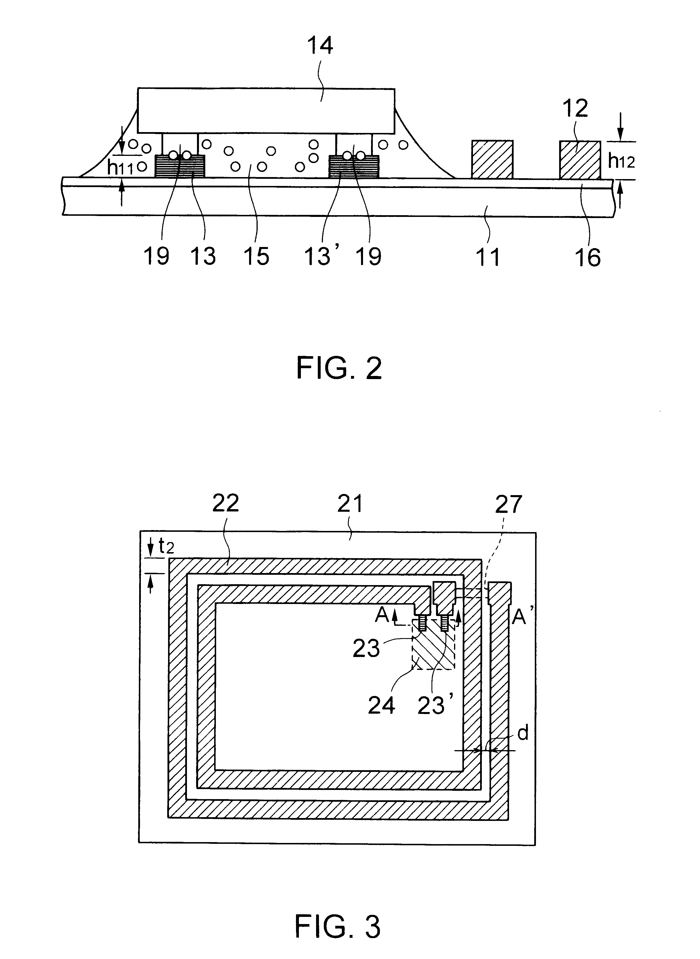
FIG. 1 is a plan view of a non-contact IC card according to the present invention, and FIG. 2 is a sectional view of an 20 IC chip mounting portion of a non-contact IC card according to the present invention (a sectional view taken along line A-A' of FIG. 1). FIG. 7 is a characteristic diagram showing the relationship between the antenna resistance of an antenna coil of FIG. 1 and a communication distance, and FIG. 8 is a schematic perspective view of an IC card communication system. The non-contact IC card comprises: an insulating substrate 11 of an insulating material, such as an epoxy resin or a polyimide resin; an antenna coil 12 of a conductor, such as aluminum or copper; IC chip connecting terminals 13 and 13' which constitute a part of the antenn...


PUM


Abstract

A non-contact IC card comprises: a substantially rectangular insulating substrate; a semiconductor chip mounted on a first face of the insulating substrate; and an antenna coil for transmitting information and for enhancing the mechanical strength of the insulating substrate, the antenna coil being arranged on the first face of the insulating substrate along the outer periphery of the first face, and the antenna coil having first and second connecting terminals which are connected to the semiconductor chip. Thus, it is possible to provide a non-contact IC card capable of enhancing the connection reliability of an IC chip mounting portion, maintaining communication characteristics, and maintaining a high mechanical strength.

Description

BACKGROUND OF THE INVENTION1. Field of the InventionThe present invention relates generally to a non-contact IC card wherein a semiconductor memory device is used as an IC chip. More specifically, the invention relates to the structure of an antenna coil which is formed in a non-contact IC card. The present invention is used for, e.g., a credit card or a commodity tag.2. Related Background ArtFIG. 9 is a plan view of a conventional non-contact IC card, and FIG. 10 is a sectional view of the non-contact IC card taken along line A-A' of FIG. 9. A quadrangular insulating substrate 1 to be an IC card substrate is made of a synthetic resin, such as a polyimide resin or an epoxy resin. The shape of the insulating substrate 1 is like a card about 5.5 by about 8.5 millimeters. An elliptical antenna coil 2 of copper or aluminum is bonded to the central portion of the major surface of the insulating substrate 1 by means of an adhesive 6. An IC chip 4 is formed at a suitable position outside o...

Claims


Application Information

Patent Timeline
Patent Type & Authority Patents(United States)
IPC IPC(8): G06K19/077G06K19/07B42D15/10H01Q7/00
CPCG06K19/07749G06K19/0775H01L2924/07811H01L2924/00011H01L2224/83385H01L2224/81385H01L2224/293H01L2224/2929H01L2224/16225H01L2224/16H01L2924/01079H01L2924/3025H01L2224/1403H01L2224/16227H01L2224/83851H01L2224/81903H01L2224/29075H01L2924/00014H01L2924/00H01L2224/14515H01L2224/45144
Inventor SUZUYA, NOBUHITO
Owner KK TOSHIBA
Why Eureka
Try Eureka