

Method for growing a solid type II-VI semiconductor material
a semiconductor material and growth method technology, applied in the growth process of crystals, basic electric elements, electrical appliances, etc., can solve the problems of high resistance, large size and high resistance, and insufficient reproduction of pulling on the other
- Summary
- Abstract
- Description
- Claims
- Application Information
AI Technical Summary
Benefits of technology
Problems solved by technology
Method used
Image

Examples
Embodiment Construction
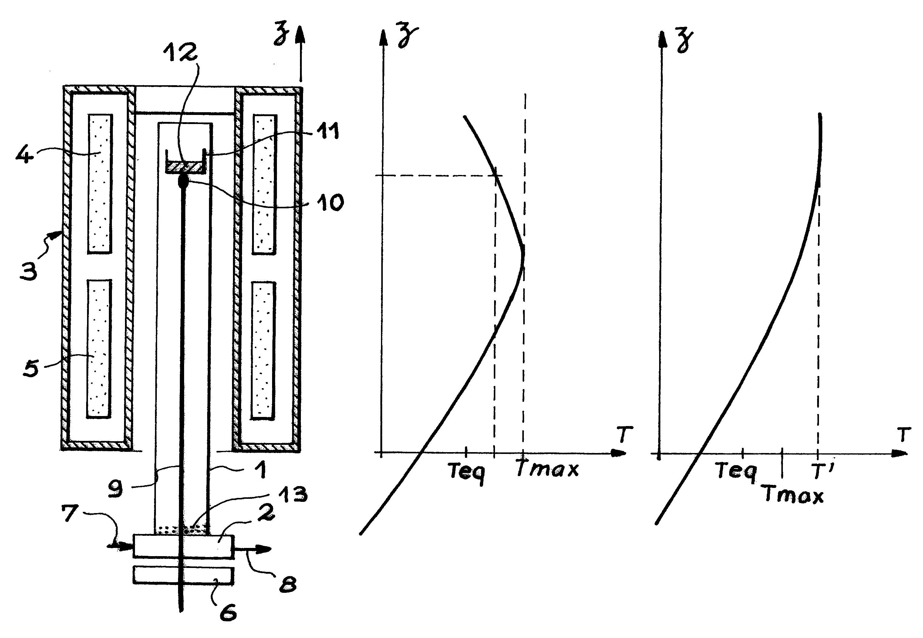
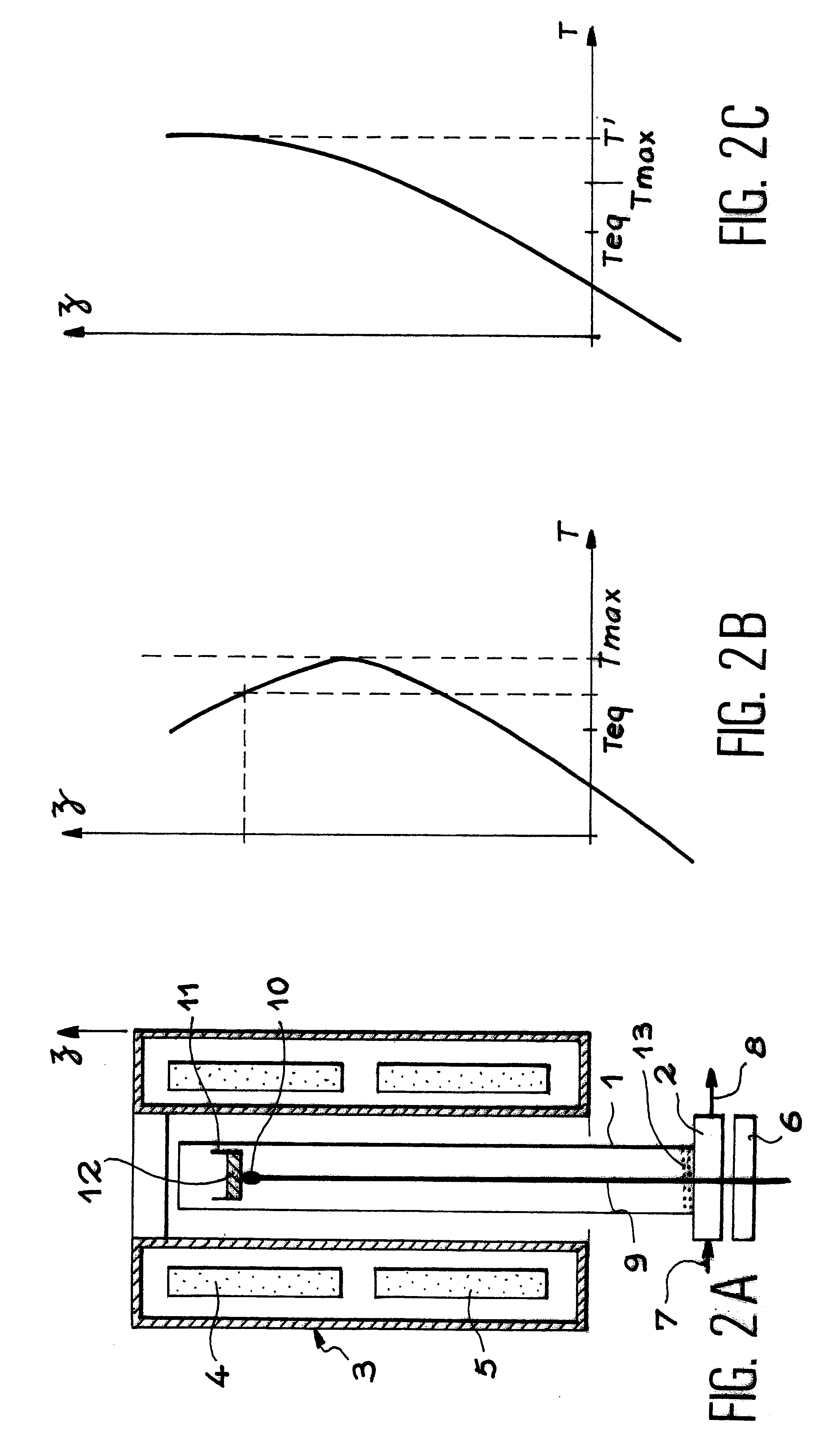
The next part of the description will focus on the growth of bulk CdTe. However, the invention is applied to the growth of other semiconductor materials of those II-VI type, including at lest one first component and a second component.
According to the invention, the crystal growth is performed in an open tube reactor which only has one temperature zone to be controlled. In the case of CdTe, it is the tellurium which will be used as a solvent.
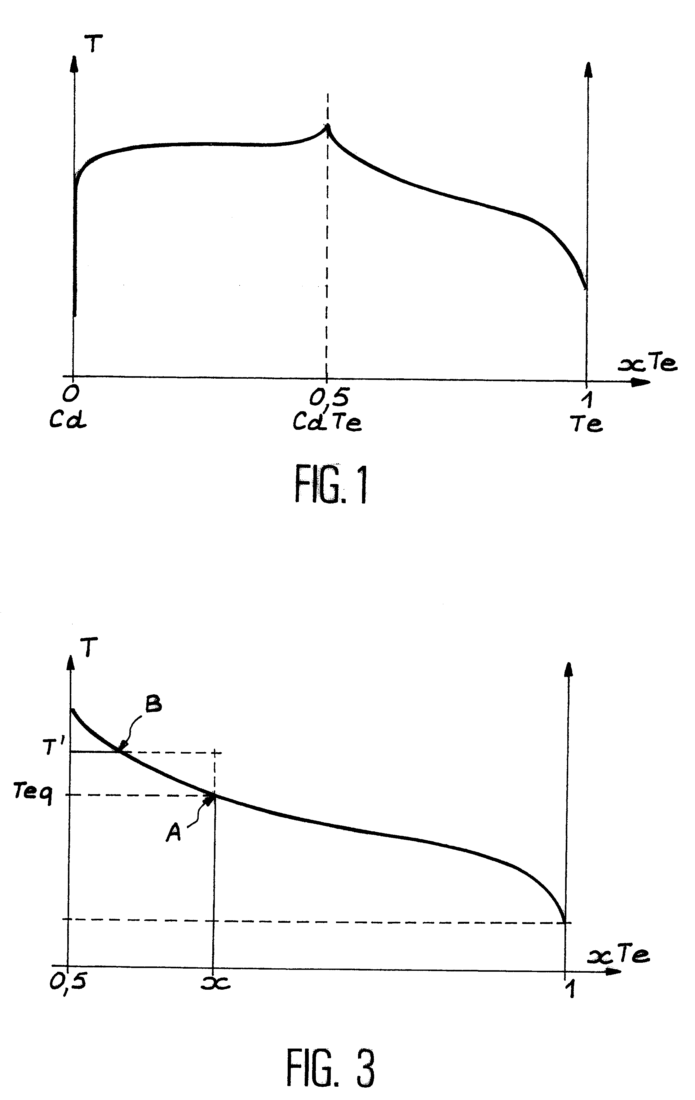
FIG. 1 shows the complete phase diagram for a mixture of CdTe according to the temperature, T. The axis of the abscissa shows the proportion of the components in the mixture. For x=0, there is only pure cadmium. For x=1, there is only pure tellurium. The diagram demonstrates that tellurium may be used more judiciously than cadmium as a solvent for the CdTe because it has a better solubility at all temperatures. Furthermore, the solutions rich in tellurium have much lower partial balance pressures than those placed on the cadmium side. For exampl...
PUM
| Property | Measurement | Unit |
|---|---|---|
| diameter | aaaaa | aaaaa |
| diameter | aaaaa | aaaaa |
| pressure | aaaaa | aaaaa |
Abstract
Description
Claims
Application Information