Wafer stage assembly, servo control system, and method for operating the same

a servo control system and stage technology, applied in the field of wafer stage assembly and wafer table servo control system, can solve the problems of delay in generating output, af/al sensor generally, and difficulty in accurately aligning the overlay circuit pattern of multi-layered integrated circuits

Inactive Publication Date: 2004-02-03
NIKON CORP
View PDF10 Cites 50 Cited by
  • Summary
  • Abstract
  • Description
  • Claims
  • Application Information

AI Technical Summary

Problems solved by technology

As the miniaturization of a circuit pattern progresses, the focus depth of the projection exposure apparatus becomes very small, making it difficult to align accurately the overlay of circuit patterns of the multi-layered integrated circuit.
However, the AF / AL sensor generally has several limitations, including, first, it only operates when wafer 68 is placed directly under projection lens assembly 78, and second, it requires significant signal processing causing a delay in generating an output.

Method used


Image

  • Wafer stage assembly, servo control system, and method for operating the same
  • Wafer stage assembly, servo control system, and method for operating the same
  • Wafer stage assembly, servo control system, and method for operating the same

Examples


Embodiment Construction

Reference will now be made in detail to several embodiments of device, system, and method consistent with the principles of the present invention, examples of which are illustrated in the accompanying drawings. The invention will be further clarified by the following examples, which are intended to be exemplary of the invention.

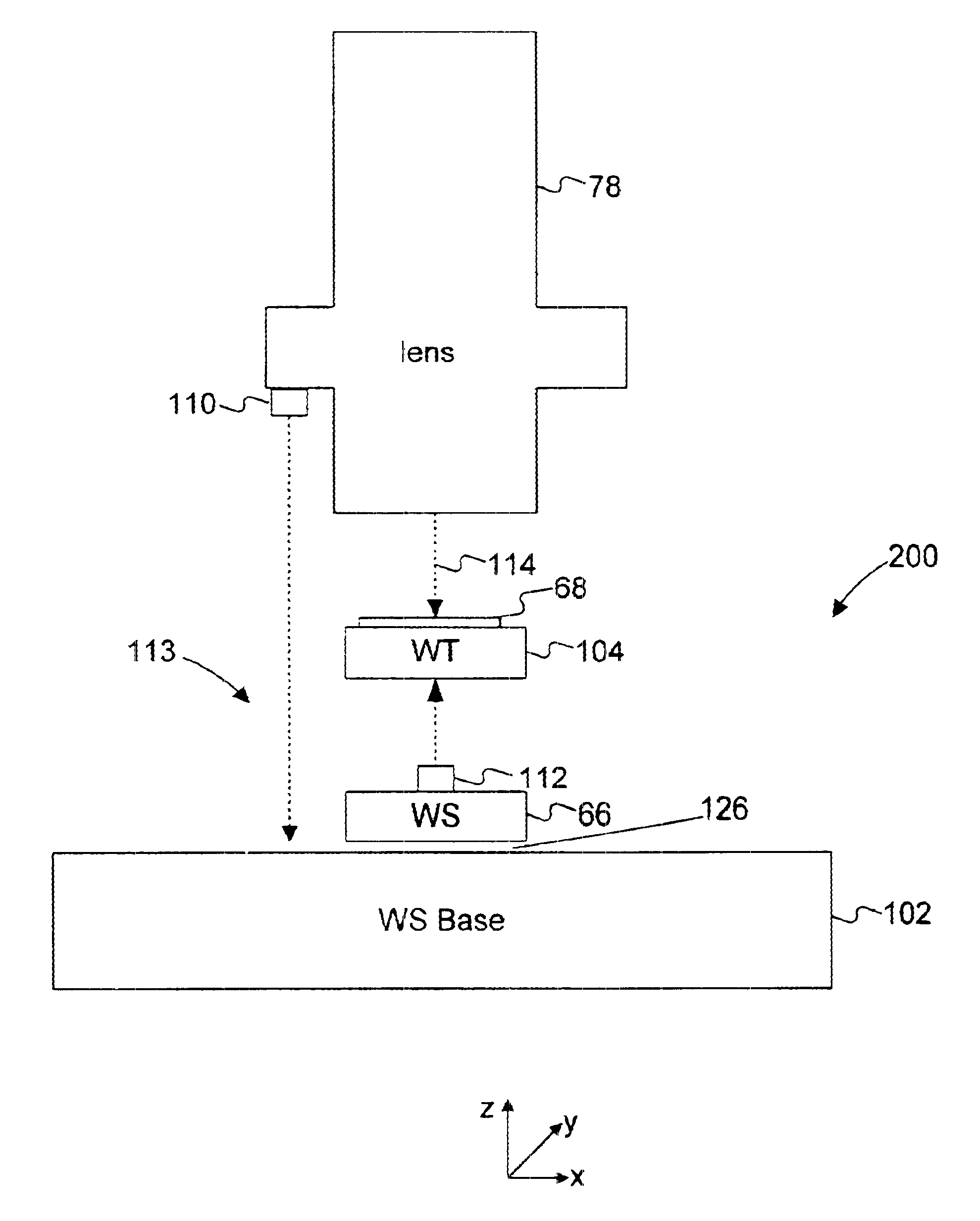
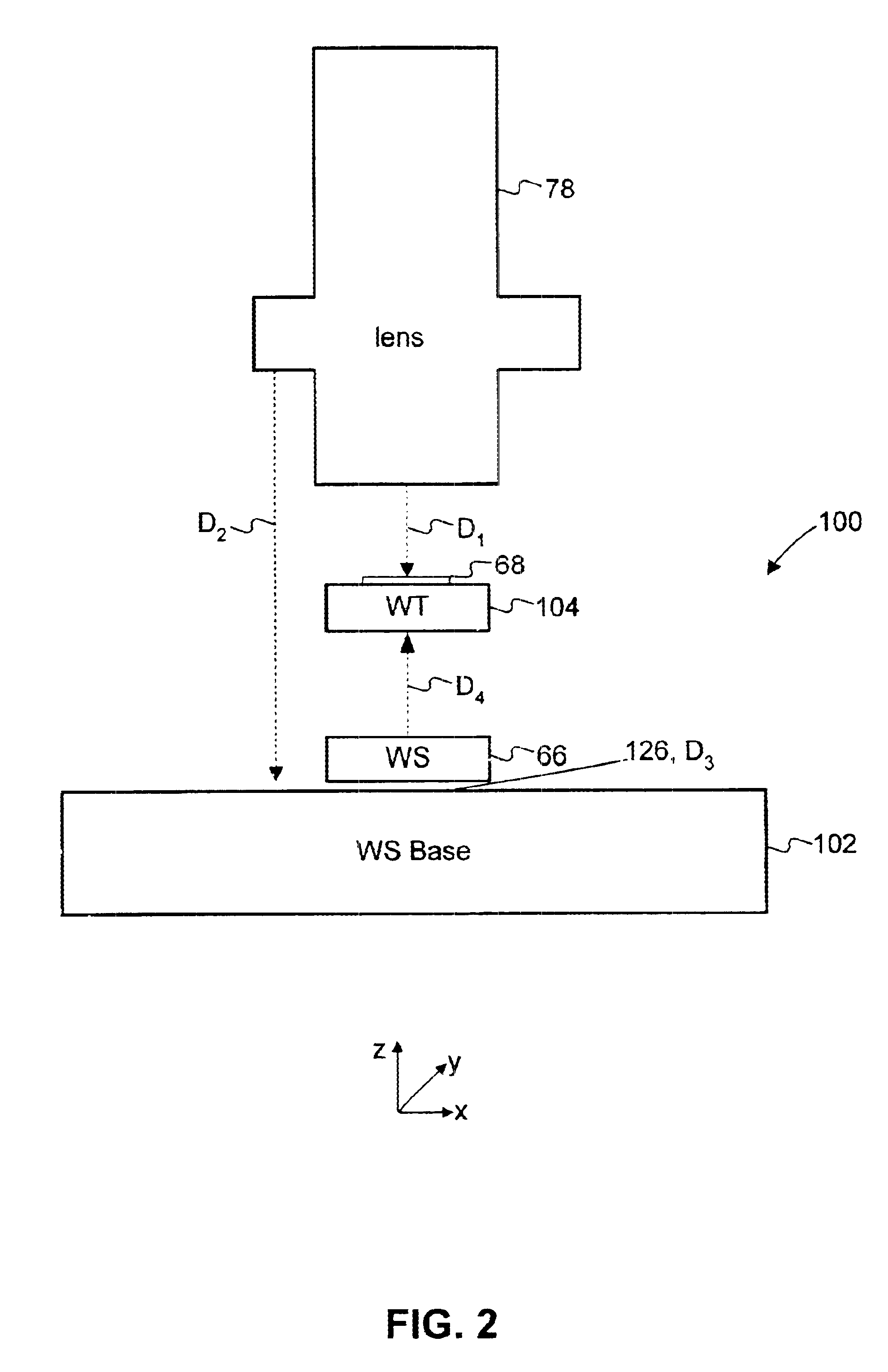
Consistent with the principles of the present invention, and as shown in FIGS. 2-4, a wafer stage assembly 100 includes a wafer table 104 to support a wafer substrate 68, a wafer stage 66, and a wafer stage base 102. Wafer stage base 102 supports wafer stage 66. A bearing 126 of pressurized fluid separates wafer stage 66 from wafer stage base 102. A set of flexures 106 connects wafer table 104 to wafer stage 66.

FIGS. 2-4 illustrate a unibody system whereby apparatus frame 72 rigidly supports wafer stage assembly 100 and projection lens system 78. A vibration isolation system 120 is provided to isolate apparatus frame 72 from internal, external, and environmen...


PUM

PropertyMeasurementUnit
wavelengthaaaaaaaaaa
distanceaaaaaaaaaa
forceaaaaaaaaaa

Abstract

A wafer stage assembly, wafer table servo control system, and method for operating the same, are provided for use in combination with a projection lens assembly in a semiconductor wafer manufacturing process. The wafer stage assembly includes a wafer stage base supporting a wafer stage to position the semiconductor wafer, a wafer table connected to the wafer stage to support the wafer, a plurality of sensors, and an actuator. The sensors include a first sensor to determine a position of an exposure point on the wafer relative to the projection lens assembly, and a second sensor to determine a position of a focal point of the projection lens assembly relative to the exposure point. To increase focusing properties of the projection lens assembly, in response to the determined positions of the exposure point and the focal point, the actuator moves the wafer table so that the exposure point substantially coincides with the focal point. The wafer table servo control system is provided to operate the wafer stage assembly. The servo control system includes a first sensor controller to generate a first position signal of an exposure point on the wafer table relative to a projection lens assembly, and a second sensor controller to generate a second position signal of a focal point of the projection lens assembly relative to the exposure point. The servo control system also includes a wafer table controller to determine and generate a correction force corresponding to the first and second position signals. The correction force is then exerted onto the wafer table to bring the exposure point to substantially coincide with the focal point.

Description

1. Field of the InventionThis invention relates to a wafer stage assembly, a wafer table servo control system and to a method for operating the same in a photolithography process to manufacture semiconductor wafers. More particularly, this invention relates to the wafer stage assembly, wafer table servo control system and method of operation to increase focusing properties of the photolithography system.2. Description of the Related ArtIn manufacturing integrated circuits using photolithography, an energy beam, such as light, is transmitted through non-opaque portions of a pattern on a reticle, or photomask, through a projection exposure apparatus, and onto a wafer of specially-coated silicon or other semiconductor material. The uncovered portions of the coating that are exposed to light are cured. The uncured coating is then removed by an acid bath. Then, the layer of uncovered silicon is altered to produce one layer of the multi-layered integrated circuit. Conventional systems use...

Claims


Application Information

Patent Timeline
Patent Type & Authority Patents(United States)
IPC IPC(8): G03F7/20G03F9/00
CPCG03F7/70716G03F9/7026
Inventor BINNARD, MICHAELUETA, TOSHIO
Owner NIKON CORP
Why Eureka
Try Eureka