Micro-device with thermal actuator

a micro-device and actuator technology, applied in the direction of thermal micromechanical switches, microstructural technology, electric/electrostrictive devices, etc., can solve the problems of pneumatic dampening, difficult technical production of the active line contact, and the delicate problem of the available power on the board of the micro-switch for this type of equipmen

Inactive Publication Date: 2004-03-09
COMMISSARIAT A LENERGIE ATOMIQUE ET AUX ENERGIES ALTERNATIVES
View PDF16 Cites 21 Cited by
  • Summary
  • Abstract
  • Description
  • Claims
  • Application Information

AI Technical Summary

Benefits of technology

To remedy the disadvantages mentioned above, a micro-device is proposed comprising conductors located on a first level and conductors located on a second level, where the conductors of the first level are supported by a deformable element which can trigger by means of an actuator with bimetallic effect; the effect of the triggering is to modify the gap between the conductors on the first level and the conductors on the second level, characterised in that the actuator with bimetallic effect consists of resistors in close and localised contact with the deformable element, and in that the resistors are able, when traversed by an electric control current, to expand sufficiently under the effect of the heat produced by the passage of the electric control current to cause, by a bimetallic effect, a triggering of the deformable element before the heat produced in the resistors has been able to propagate in the deformable element.
The resistors may include at least one layer deposited in the shape of a wave. This leads to improved efficiency for the actuator.

Problems solved by technology

The design of a microswitch for this type of equipment is confronted with the delicate problem of the on-board available power to activate the microswitches.
This causes a pneumatic dampening.
Moreover, technical production of the active line's contact is very difficult and the large number of electrodes involved tends to cause disturbances in the control on the radio frequency signal conveyed by the active line.

Method used


Image

  • Micro-device with thermal actuator
  • Micro-device with thermal actuator
  • Micro-device with thermal actuator

Examples


Embodiment Construction

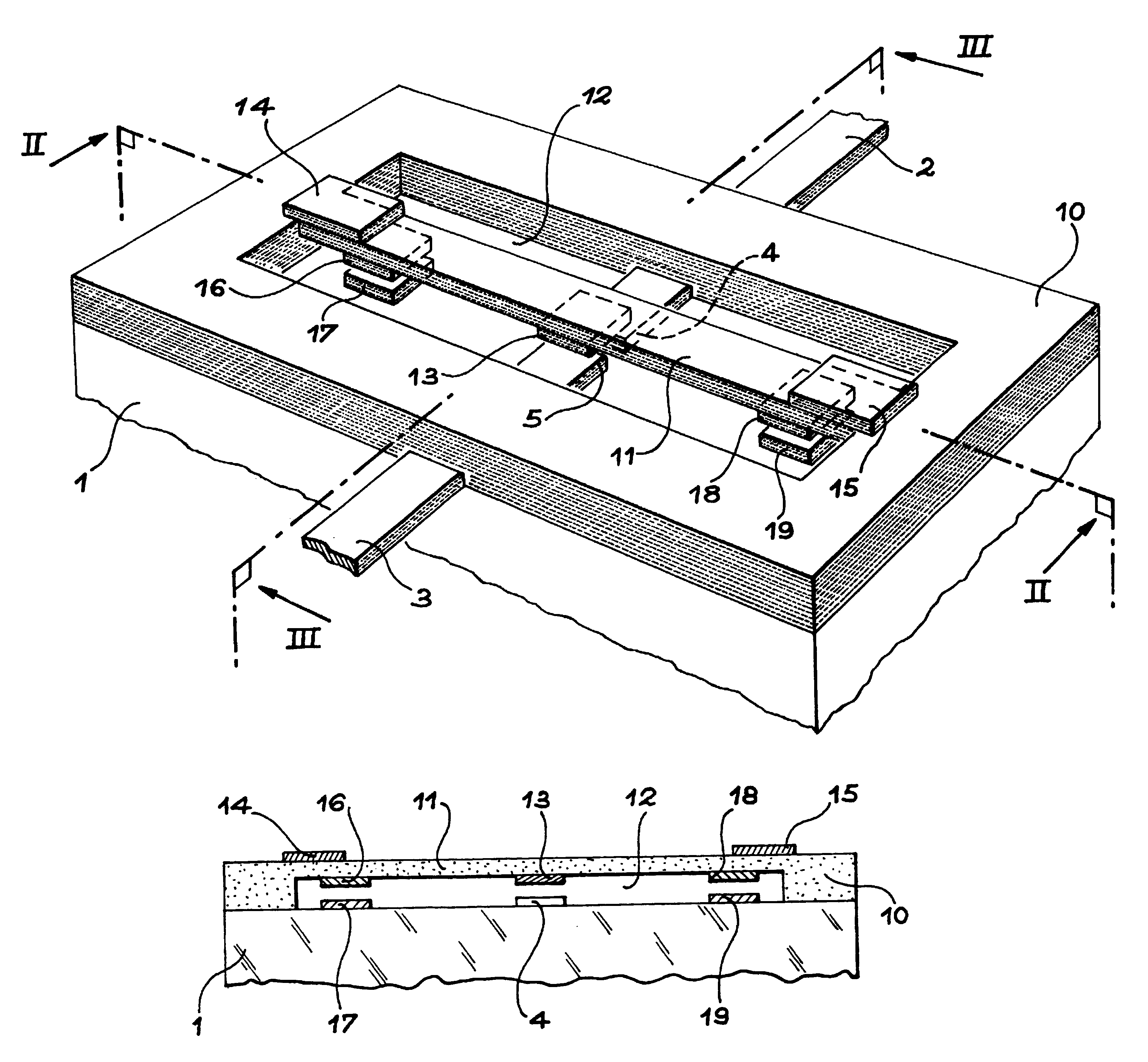
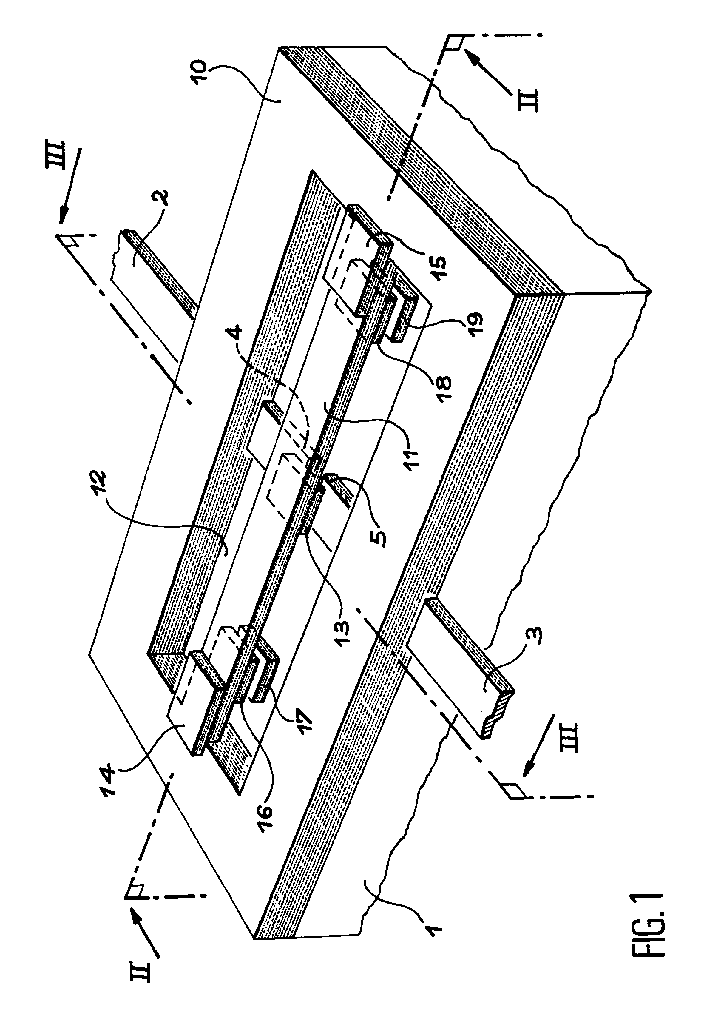
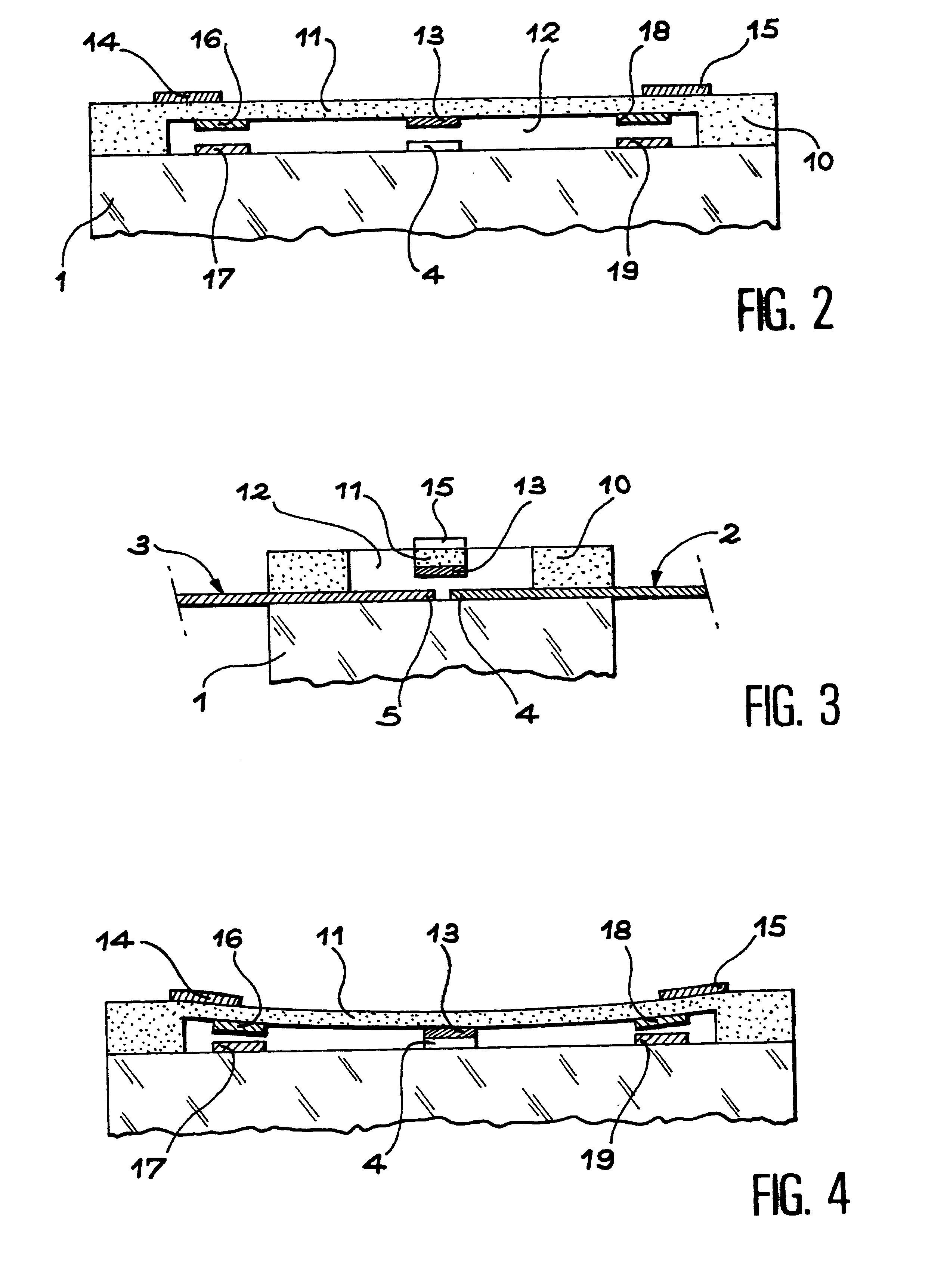
FIG. 1 (perspective view) and FIGS. 2 and 3 (section views) illustrate a microswitch according to the present invention.

This microswitch is produced on a substrate 1, for example made from silicon, silica, glass or quartz. Substrate 1 supports a first section of line 2 terminated by a contact 4 and a second section of line 3 terminated by a contact 5. Contacts 4 and 5 are simply separated by a small interval.

Substrate 1 supports one or more layers, made from an electrical insulating material, designated as single reference 10 and from which a deformable element has been produced in the form of member 11 (for example made from silicon nitrite or silicon oxide) able to be deformed in a cavity 12 of layer 10 revealing the substrate 1 and contacts 4 and 5. Member 11 has, on the side of cavity 12, a conductive block 13 able to form an electrical link between contacts 4 and 5 when member 11 deflects in cavity 12. This microswitch may be achieved by the process divulged in document FR-A-2 ...


PUM


Abstract

The invention relates to a microswitch containing conductors located on a first level and conductors located on a second level, where the conductors on the first level are supported by a deformable element which can switch by means of an actuator with a bimetallic effect, and where the effect of this switching is that the gap between the conductors on the first level and the conductors on the second level is modified, characterised in that the actuator with a bimetallic effect consists of resistors in close and localised contact with the deformable element, and in that the resistors are capable, when traversed by an electric control current, of expanding sufficiently under the effect of the heat produced by the passage of the electric command current to cause, by the bimetallic effect, the deformable element to trigger before the heat produced in the resistors has been able to propagate into the deformable element.

Description

The present invention relates to a micro-device with an element which deforms under the effect of a thermal actuator. This micro-device may constitute a microswitch which is particularly well-suited to switching of radio frequency signals.STATE OF PRIOR TECHNOLOGYMicroswitches are micro-devices which are increasingly used in modern electronic devices one of the major characteristics of which is their increasingly small size. This is the case, notably, with mobile telephones. The design of a microswitch for this type of equipment is confronted with the delicate problem of the on-board available power to activate the microswitches. Current microswitches must be able to be controlled using low voltages (3V for example) and over very short times.The document "Micromechanical relay with electrostatic actuation and metallic contacts" by M. -A. GRETILLAT et al., Transducers '99, Jun. 7-10, 1999, Sendai, Japan, divulges an electrostatically-controlled microswitch requiring a control of arou...

Claims


Application Information

Patent Timeline
Patent Type & Authority Patents(United States)
IPC IPC(8): H01H1/00H01H61/00H01H61/02B81B3/00F03G7/06H01H1/04H01H37/52H01H59/00H01H61/01
CPCH01H1/0036H01H61/02H01G5/16H01H2001/0063H01H2037/008H01H2061/006
Inventor CHARVET, PIERRE-LOUISDUFOUR, MICHEL
Owner COMMISSARIAT A LENERGIE ATOMIQUE ET AUX ENERGIES ALTERNATIVES
Why Eureka
Try Eureka