Methods for silicon oxide and oxynitride deposition using single wafer low pressure CVD

a technology of oxynitride and silicon oxide, which is applied in the direction of chemical vapor deposition coating, liquid surface applicator, coating, etc., can solve the problems of depletion effect of state of art system, difficult to obtain uniform thickness for wafers in a batch and batch to batch,

Inactive Publication Date: 2004-03-30
APPLIED MATERIALS INC
View PDF0 Cites 86 Cited by
  • Summary
  • Abstract
  • Description
  • Claims
  • Application Information

AI Technical Summary

Benefits of technology

These films are formed using well known techniques such as CVD. Low-pressure chemical vapor deposition (LPCVD) is a special case of a CVD process, typically used for front end of line (FEOL) dielectric film deposition. In a CVD process, a given composition and flow rate of reactant gases and diluent carrier gases are introduced into a reaction chamber. The gas species move to a substrate and the reactants are adsorbed on the substrate. The atoms undergo migration and film-forming chemical reactions and a film (e.g., silicon oxide) is deposited on the substrate. The gaseous byproducts of the reaction and removed from the reaction chamber. Energy to drive the reactions can be supplied by several methods, e.g. thermal, light and radio frequency, catalysis, or plasma. A conventional CVD system typically contain gas sources, gas feed lines, mass-flow controllers, a reaction chamber, a method for heating substrates onto which the film is to be deposited, and temperature sensors. A conventional LPCVD system is similar to the CVD system except that temperature is the primary driver for the reaction of source gases.

Problems solved by technology

The state of the art system suffers a disadvantage called "depletion effects."
As a result, uniform thickness is difficult to obtain for the wafers in a batch and from batch to batch.

Method used


Image

  • Methods for silicon oxide and oxynitride deposition using single wafer low pressure CVD
  • Methods for silicon oxide and oxynitride deposition using single wafer low pressure CVD
  • Methods for silicon oxide and oxynitride deposition using single wafer low pressure CVD

Examples


Embodiment Construction

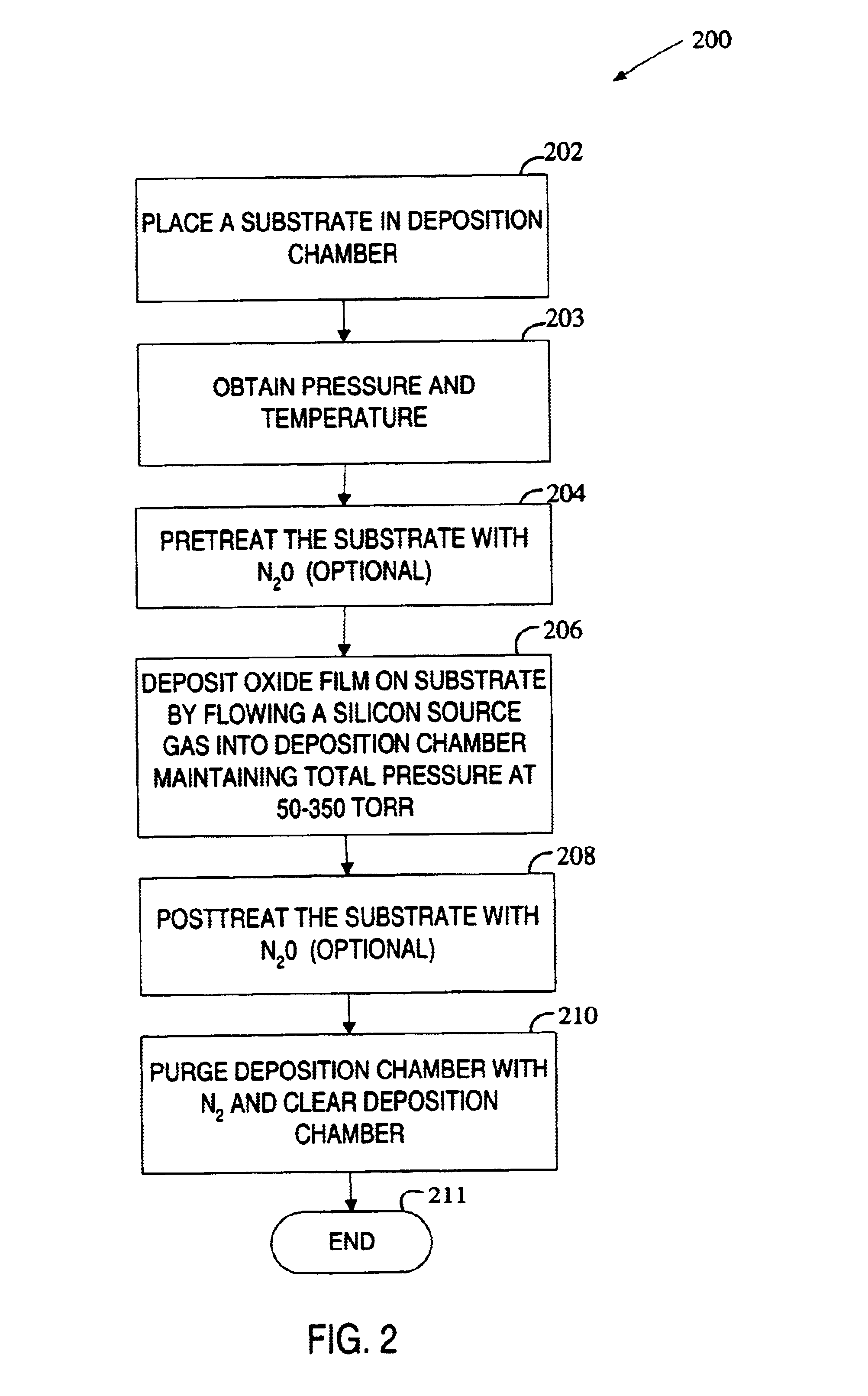
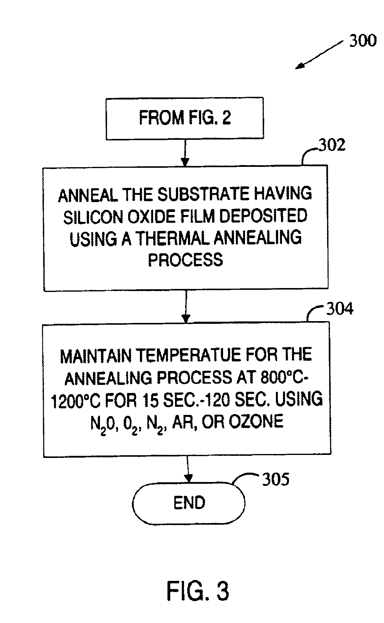
The present invention is a novel method of forming a low temperature, medium temperature and high temperature silicon oxide, or silicon oxynitride film. In the following description, for purposes of explanation, numerous specific details are set forth in order to provide a thorough understanding of the present invention. It will be evident, however, to one skilled in the art, that the present invention may be practiced without these specific details. In other instances, specific apparatus structures and methods have not been described so as not to obscure the present invention. The following description and drawings are illustrative of the invention and are not to be construed as limiting the invention.

The following sections describe novel methods to deposit a low temperature, medium temperature, or high temperature film (e.g., silicon oxide and a silicon oxynitride film). The low temperature film is formed with a deposition temperature ranging from 300.degree. C. to 600.degree. C.;...


PUM

PropertyMeasurementUnit
temperatureaaaaaaaaaa
pressureaaaaaaaaaa
total pressureaaaaaaaaaa

Abstract

An oxide and an oxynitride films and their methods of fabrication are described. The oxide or the oxynitride film is grown on a substrate that is placed in a deposition chamber. A silicon source gas (or a silicon source gas with a nitridation source gas) and an oxidation source gas are decomposed in the deposition chamber using a thermal energy source. A silicon oxide (or an oxynitride) film is formed above the substrate wherein total pressure for the deposition chamber is maintained in the range of 50 Torr to 350 Torr and wherein a flow ratio for the silicon source gas (or the silicon source gas with the nitridiation source gas) and the oxidation source gas is in the range of 1:50 to 1:10000 during a deposition process.

Description

1. Field of the InventionThe present invention relates to the field of semiconductor integrated circuit manufacturing and more specifically to medium temperature deposition and high temperature deposition of silicon oxide films and methods of fabrication of these oxide films.2. Discussion of Related ArtChemical vapor deposited (CVD) SiO.sub.2 films and their binary and ternary silicates (generally referred to as oxide films) have wide use in fabrication of integrated circuits such as microprocessors and memories. These films are used as insulation between polysilicon and metal layers, between metal layers in multilevel metal systems, as diffusion sources, as diffusion and implantation masks, as spacers, and as final passivation layers. Acceptable deposited oxide film processes provide uniform thickness and composition, low particulate and chemical contamination, good adhesion to the substrate, and high throughput for manufacturing.These films are formed using well known techniques s...

Claims


Application Information

Patent Timeline
Patent Type & Authority Patents(United States)
IPC IPC(8): C23C16/56C23C16/40C23C16/30C23C16/44C23C16/42C23C16/455H01L21/316H01L21/318
CPCC23C16/308C23C16/401C23C16/45512C23C16/56C23C16/40H01L21/0262C23C16/44
Inventor SUBRAMONY, JANARDHANAN ANANDYOKOTA, YOSHITAKAIYER, RAMASESHAN SURYANARAYANANLUO, LEECHEN, AIHUA
Owner APPLIED MATERIALS INC
Why Eureka
Try Eureka