Edge contact loadcup

a load cup and edge contact technology, applied in the field of load cups, can solve the problems of wafer damage and particulate contamination, and achieve the effect of reducing the possibility of damage to the wafer and reducing the risk of contamination

Inactive Publication Date: 2004-04-06
APPLIED MATERIALS INC
View PDF10 Cites 29 Cited by
  • Summary
  • Abstract
  • Description
  • Claims
  • Application Information

AI Technical Summary

Benefits of technology

The disadvantages associated with the prior art are overcome by the present invention of an edge contact loadcup for positioning a semiconductor wafer in a fixture such as a retaining ring of a Chemical Mechanical Polishing system. More specifically, the edge contact loadcup or loadcup comprises a cone and a workpiece (or wafer) chuck connected to one another by a flexure. The flexure prevents lateral movement of the workpiece chuck in relation to cone, while permitting axial movement between the wafer chuck and the cone.

Problems solved by technology

Additionally, as the process of alignment requires both contact of the alignment jaws to the wafer and the physical sliding of the wafer upon the pedestal, both actions incur the possibility of wafer damage and particulate contamination.

Method used


Image

  • Edge contact loadcup
  • Edge contact loadcup
  • Edge contact loadcup

Examples


Embodiment Construction

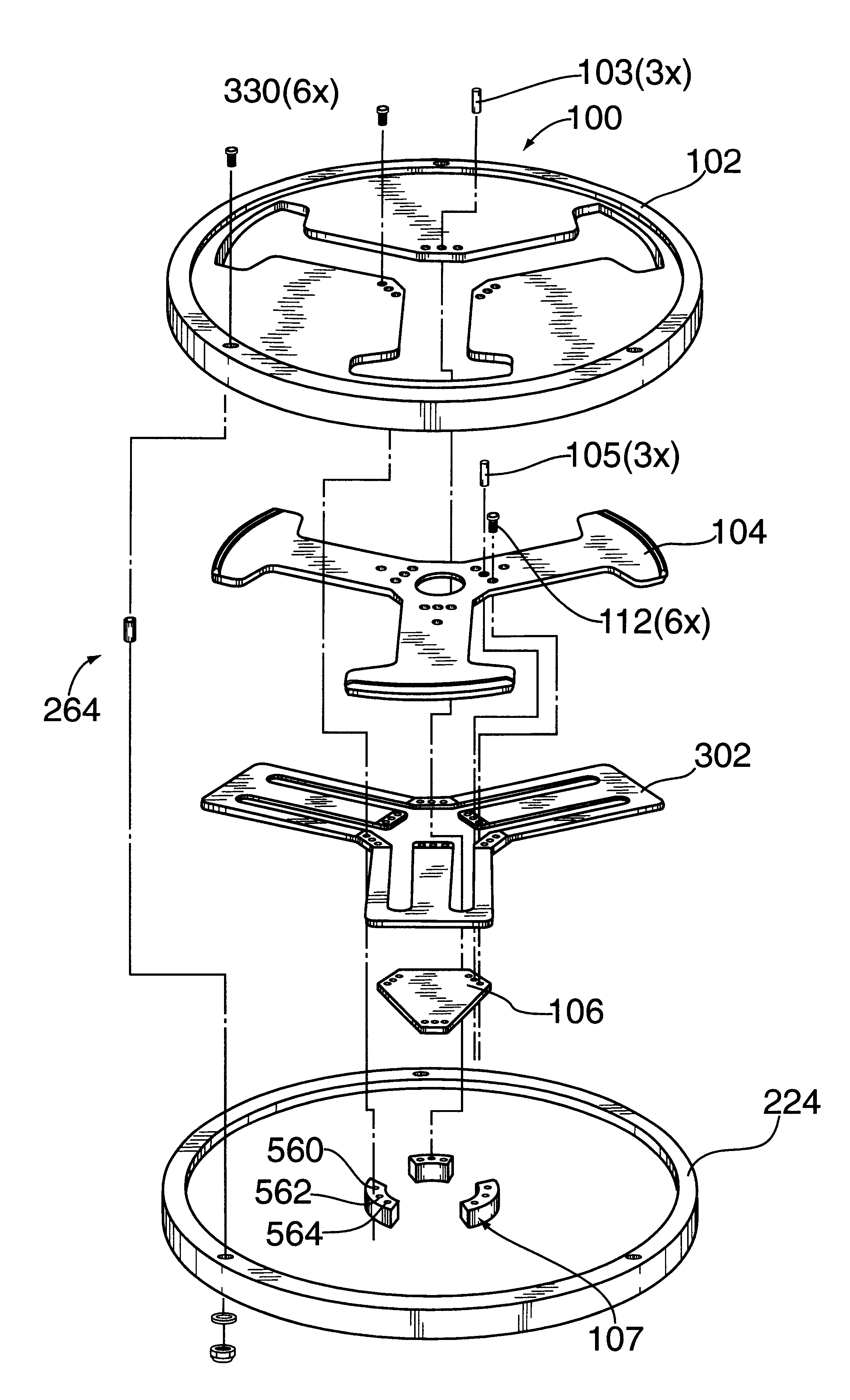
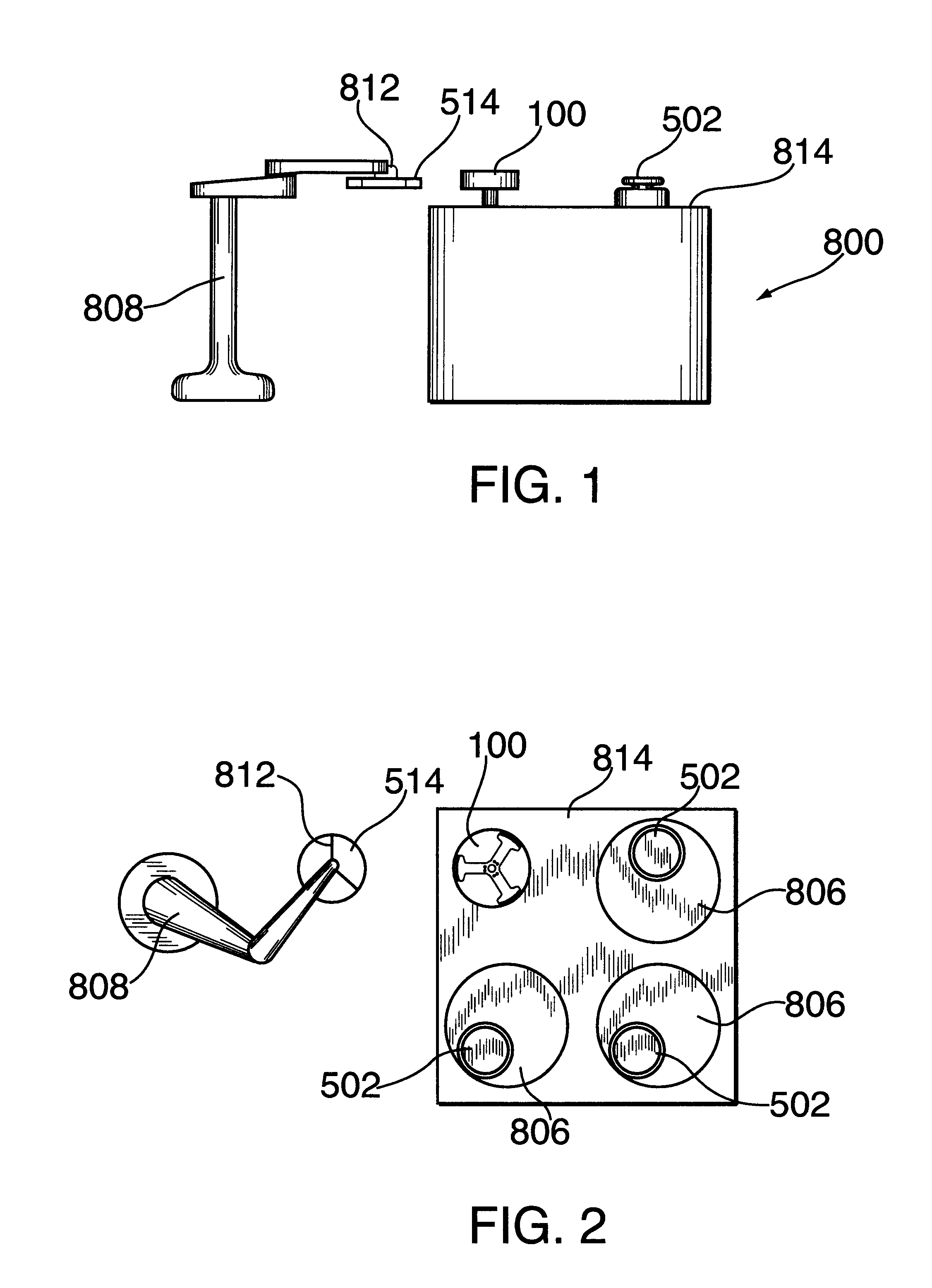
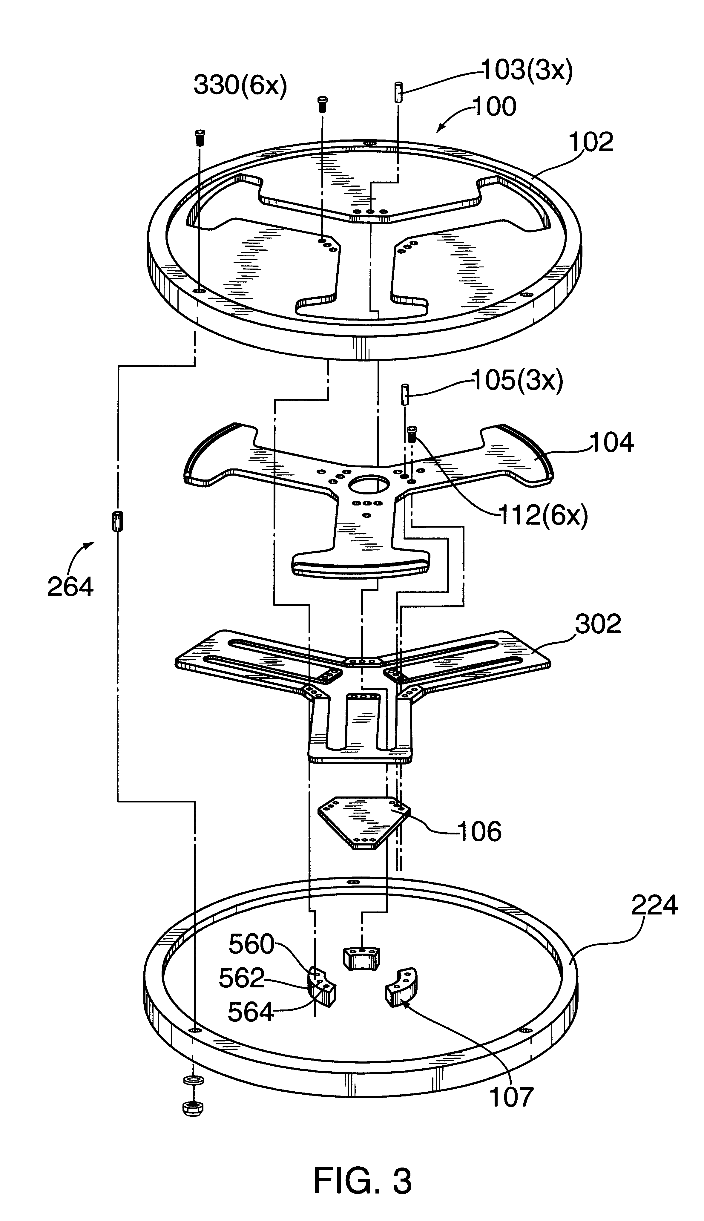
A chemical mechanical polisher 800 is schematically depicted in FIG. 1 and FIG. 2. The reader is encouraged to simultaneously refer to both FIG. 1 and FIG. 2 for the best understanding of the invention. The polisher 800 has a plurality of polishing stations 806, i.e. three, and an edge contact loadcup 100. The polishing stations 806 and the loadcup 100 are accessible from a top surface 814 of the polisher 800. Each polishing station 806 is serviced by a retaining ring 502 that moves between the loadcup 100 and the polishing stations 806. For clarity, the assembly, a polishing head carousel, that supports and moves the retaining ring 502 is not shown in FIG. 1 and FIG. 2.

A wafer 514 is transferred between the polisher 800 and other systems or cassettes (not shown) via a wafer transfer mechanism (or robot) 808. The transfer mechanism 808 has a gripper-like device 812 which holds the wafer 514 during transfer, and sets the wafer 514 into the loadcup 100. After the loadcup 100 receives ...


PUM


Abstract

A semiconductor wafer processing apparatus, more specifically, an edge contact loadcup for locating a semiconductor workpiece or wafer into a chemical mechanical retaining ring utilizing a cone, wafer chuck and flexure. The cone aligns the wafer concentrically to the retaining ring. The wafer chuck, inside the cone, is restrained from moving laterally in respect to the cone by the flexure. The wafer, which is supported by the wafer chuck, is moved into the retaining ring by the wafer chuck after the cone has become aligned with the retaining ring. An adjustment mechanism is provided to ensure the co-planar orientation of the wafer and fixture. Other embodiments include a sensor for detecting the presence of the wafer on the chuck, and in the cone, and minimizes particulate contamination to the wafer.

Description

BACKGROUND OF THE DISCLOSURE1. Field of InventionThe present invention relates generally to a semiconductor wafer chemical mechanical polishing system. More specifically, the invention relates to a loadcup for positioning a workpiece or semiconductor wafer into a retaining ring of a chemical mechanical polishing system.2. Background of Prior ArtIn semiconductor wafer processing, the use of chemical mechanical polishing, or CMP, has gained favor due to the enhanced ability to stack multiple feature layers on a semiconductor workpiece, or wafer. As the demand for polishing wafers as part of a semiconductor fabrication process increases, the requirement for higher processing rates while minimizing risk of wafer damage and contamination has correspondingly experienced greater urgency for improvement.Two such CMP systems that address these issues are described in a patent to Perlov et al. (U.S. Pat. No. 5,804,507, issued Sep. 8, 1998) and in a patent to Tolles et al. (U.S. Pat. No. 5,738...

Claims


Application Information

Patent Timeline
Patent Type & Authority Patents(United States)
IPC IPC(8): B24B41/00B24B37/04H01L21/67H01L21/687B24B37/34H01L21/304H01L21/683
CPCB24B37/345B24B41/005H01L21/68785
Inventor TOBIN, JIM
Owner APPLIED MATERIALS INC
Why Eureka
Try Eureka