
SCR devices in silicon-on-insulator CMOS process for on-chip ESD protection

a technology of silicon-on-insulator and cmos, applied in the direction of semiconductor devices, semiconductor/solid-state device details, electrical apparatus, etc., can solve the problems of not being able to protect gate oxides, being susceptible to electrostatic discharge events, and being triggered by substrate noise accidentally

Inactive Publication Date: 2004-06-15
TRANSPACIFIC IP LTD
View PDF29 Cites 56 Cited by
  • Summary
  • Abstract
  • Description
  • Claims
  • Application Information

AI Technical Summary

Benefits of technology

The proposed SCR structure effectively protects integrated circuits from ESD events by reducing turn-on time and preventing accidental triggering, providing enhanced ESD protection in SOI CMOS technology.

Problems solved by technology

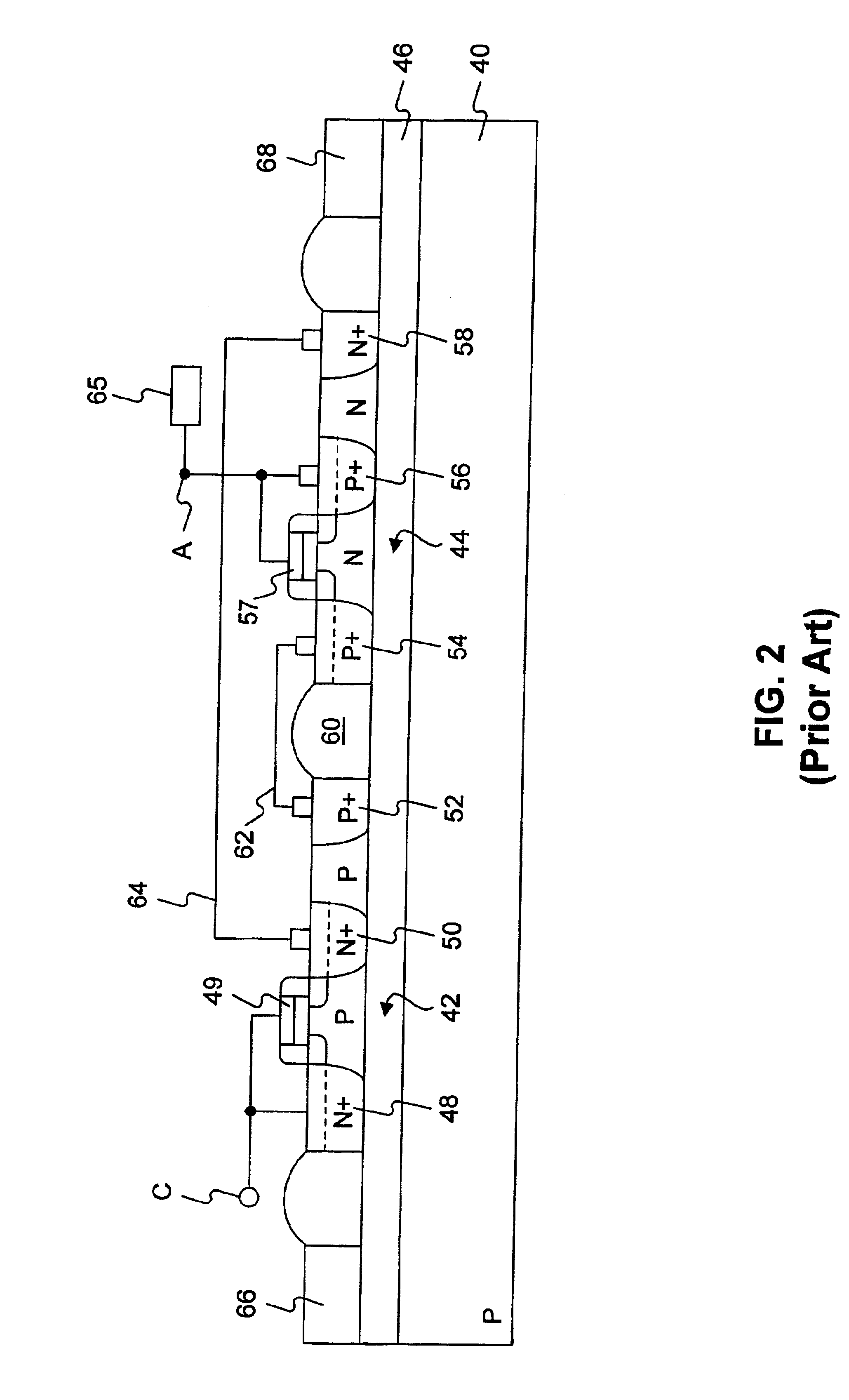
However, the SOI CMOS technology is still susceptible to an electrostatic discharge (ESD) event due to poor thermal conductivity of the insulator, e.g., buried oxide, and the floating body effect from active devices being formed over the insulator instead of a semiconductor substrate.
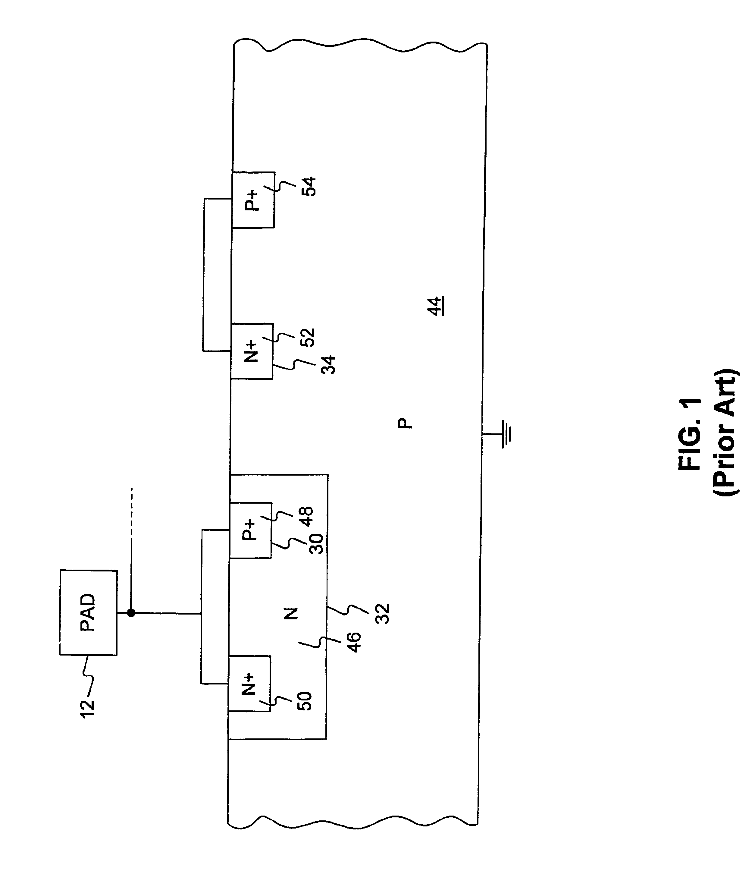
A conventional SCR device has a switching voltage of more than 30 volts in sub-micron CMOS processes, and therefore is not suitable to protect gate oxides in a sub-micron CMOS technology. FIG. 1 is a reproduction of FIG. 3 of U.S. Pat. No. 5,012,317 to Rountre, entitled "Electrostatic Discharge Protection Circuit."
However, a disadvantage of the SCR structure shown in FIG. 1 is its susceptibility to being accidentally triggered by substrate noise.

Method used


Image

  • SCR devices in silicon-on-insulator CMOS process for on-chip ESD protection
  • SCR devices in silicon-on-insulator CMOS process for on-chip ESD protection
  • SCR devices in silicon-on-insulator CMOS process for on-chip ESD protection

Examples


Embodiment Construction

1. Field of the Invention

This invention pertains in general to a semiconductor device and, more particularly, to an electrostatic discharge protection circuit incorporating a silicon controlled rectifier in a silicon-on-insulator semiconductor device.

2. Background of the Invention

Recent advances in integrated circuits have included further development of a silicon-on-insulator (SOI) technology. An SOI technology uses an insulating substrate to improve process characteristics such as speed and latch-up susceptibility. There are two types of SOI processes, fully-depleted and partially-depleted.

In an SOI complementary metal-oxide semiconductor (CMOS) technology, an independent and isolated n-type metal-oxide semiconductor (NMOS) transistor may be provided next to a p-type MOS (PMOS) transistor, and vice versa, because the NMOS and PMOS transistors are electrically isolated from each other and from the underlying silicon substrate. The main advantage of the SOI CMOS technology includes ...


PUM


Abstract

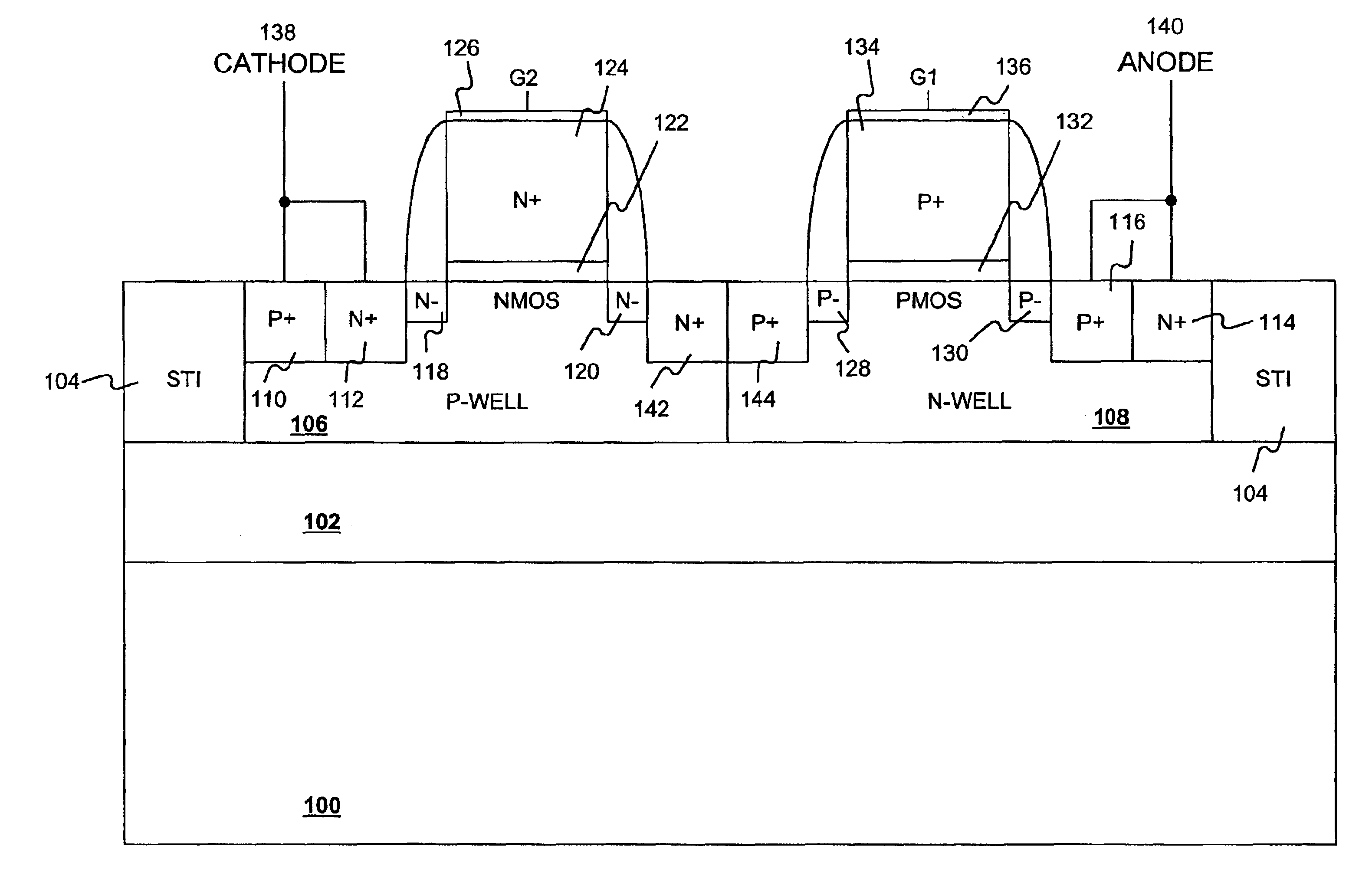
A silicon-on-isolator CMOS integrated circuit device includes a semiconductor substrate, an isolation layer formed over the semiconductor substrate, an n-type MOS transistor having a gate, a drain region, and a source region formed over the isolation layer, and a p-type MOS transistor having a gate, a drain region, and a source region formed over the isolation layer and contiguous with the n-type MOS transistor, wherein the n-type MOS transistor and the p-type MOS transistor form a silicon controlled rectifier to provide electrostatic discharge protection.

Description

DESCRIPTION OF THE INVENTION1. Field of the InventionThis invention pertains in general to a semiconductor device and, more particularly, to an electrostatic discharge protection circuit incorporating a silicon controlled rectifier in a silicon-on-insulator semiconductor device.2. Background of the InventionRecent advances in integrated circuits have included further development of a silicon-on-insulator (SOI) technology. An SOI technology uses an insulating substrate to improve process characteristics such as speed and latch-up susceptibility. There are two types of SOI processes, fully-depleted and partially-depleted.In an SOI complementary metal-oxide semiconductor (CMOS) technology, an independent and isolated n-type metal-oxide semiconductor (NMOS) transistor may be provided next to a p-type MOS (PMOS) transistor, and vice versa, because the NMOS and PMOS transistors are electrically isolated from each other and from the underlying silicon substrate. The main advantage of the S...

Claims


Application Information

Patent Timeline
Patent Type & Authority Patents(United States)
IPC IPC(8): H01L27/12H01L27/02
CPCH01L27/0262H01L27/1203
Inventor KER, MING-DOUHUNG, KEI-KANGCHANG, CHYH-YIH
Owner TRANSPACIFIC IP LTD
Learn More