

Surface emitting semiconductor laser and surface emitting semiconductor laser array
a laser array and semiconductor technology, applied in the direction of laser cooling arrangement, laser output parameters control, laser details, etc., can solve the problems of large amount of tensile strain in the semiconductor deposit, difficult to control the polarization direction of laser light, and light intensity variation
- Summary
- Abstract
- Description
- Claims
- Application Information
AI Technical Summary
Benefits of technology
Problems solved by technology
Method used
Image

Examples
second embodiment
(Second Embodiment)
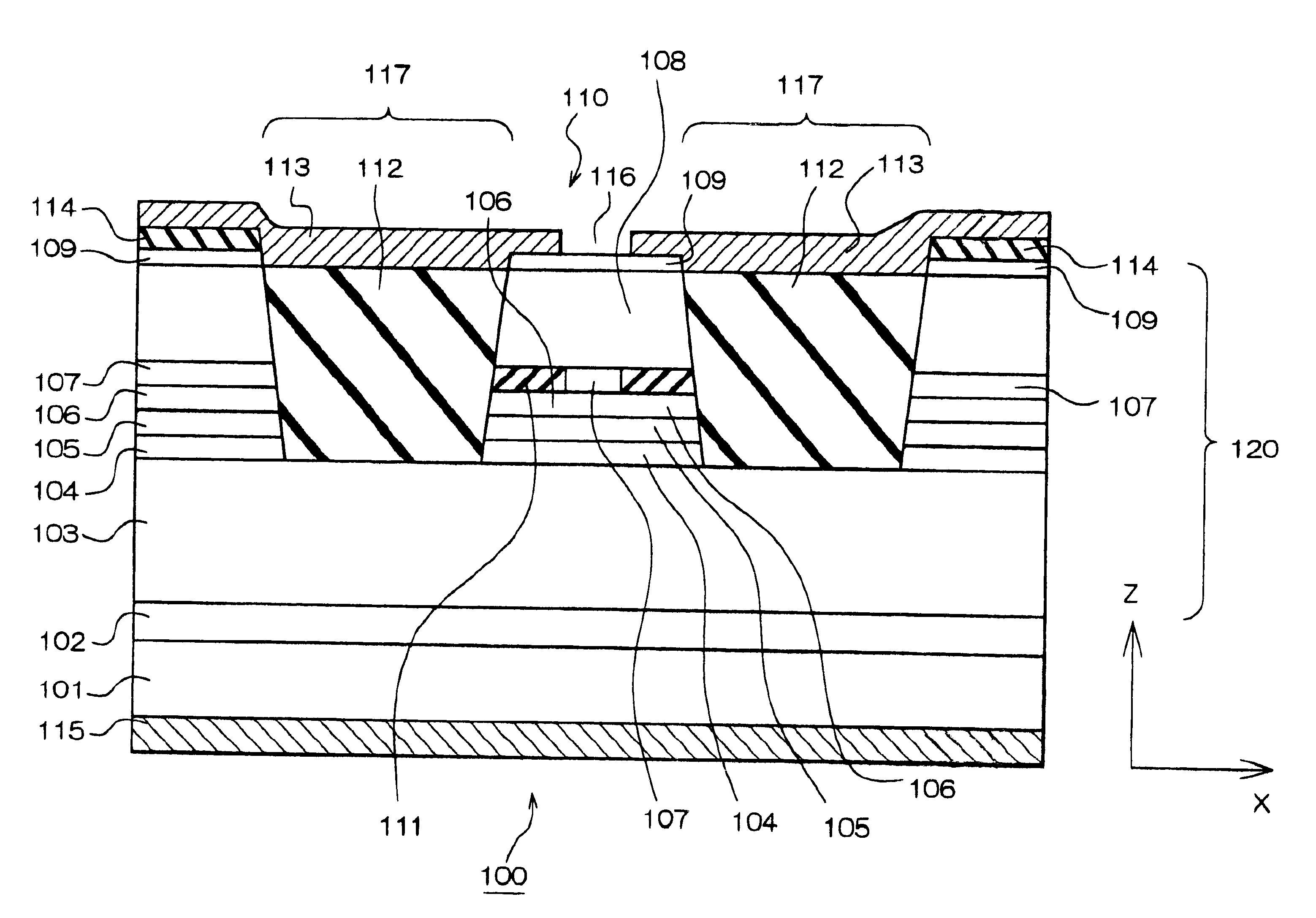
1. Device Structure
FIG. 9 is a plan view schematically showing a major portion of a surface emitting laser 200 according to a second embodiment of the present invention from the side facing a light emitting aperture.
first embodiment
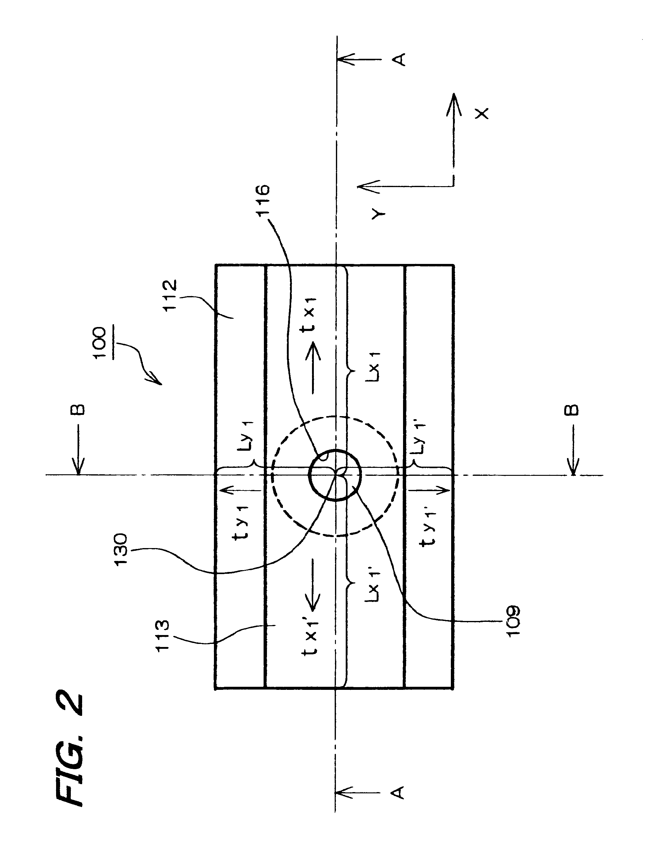
The first embodiment illustrates the case where the planar configuration of the insulating layer 112 in the surface emitting laser is rectangular. The planar configuration of the insulating layer 112 is not limited to this. The planar configuration of an insulating layer 212 in the surface emitting laser 200 according to the second embodiment is elliptical. Moreover, the planar configuration of the insulating layer 212 may be polygonal such as diamond-shaped, triangular, hexagonal, or octagonal.
In the surface emitting laser 100 according to the first embodiment, the insulating layer 112 is formed in the groove 117. In the surface emitting laser 200 according to the second embodiment, the insulating layer 212 is formed on the lower mirror 103 by patterning.
2. Device Fabrication Process
The method of fabricating the surface emitting laser according to the second embodiment is almost the same as that for the surface emitting laser according to the first embodiment. The difference betwee...
third embodiment
(Third Embodiment)
1. Device Structure
FIG. 10 is a plan view schematically showing a major portion of a surface emitting laser 300 according to a third embodiment of the present invention from the side facing a light emitting aperture. FIG. 11 is a view schematically showing the cross section of the surface emitting laser 300 shown in FIG. 10 along the line C--C. FIG. 12 is a view schematically showing the cross section of the surface emitting laser 300 shown in FIG. 10 along the line D--D.
The structure of the surface emitting laser according to the third embodiment is similar to that of the surface emitting laser 100 according to the first embodiment and that of the surface emitting laser 200 according to the second embodiment. The structure of the surface emitting laser according to the third embodiment is the same as that of the surface emitting laser 100 according to the first embodiment in that the planar configuration of an insulating layer 312 is rectangular. The structure of ...
PUM
 Abstract
Description
Claims
Application Information