Method for selective trimming of gate structures and apparatus formed thereby

a gate structure and selective trimming technology, applied in the direction of basic electric elements, semiconductor/solid-state device manufacturing, electric apparatus, etc., can solve the problems of increasing the risk of producing a distorted or defective gate conductor, the misalignment of device components, and the failure of the device, so as to reduce the sheet resistance and reduce the sheet resistance

Inactive Publication Date: 2004-07-06
INT BUSINESS MASCH CORP
View PDF29 Cites 10 Cited by
  • Summary
  • Abstract
  • Description
  • Claims
  • Application Information

AI Technical Summary

Benefits of technology

Referring to FIGS. 1 and 2, a preferred method 100 for forming transistor gate structures is shown. In step 110 of method 100, a wafer portion 700, as shown in FIG. 3, is fabricated by forming isolation structures 790 in a semiconductor substrate 780 followed by formation of a layer of gate oxide on semiconductor substrate 780 and formation of a layer of polysilicon for a gate conductor on the layer of gate oxide. The layers are then patterned, removing unneeded portions and leaving gate oxide portion 730 and polysilicon portion 740. In step 120 of method 100, polysilicon portion 740 may be trimmed to scale down its dimensions so that the resulting gate conductor will be smaller and the associated field effect transistors (FETs) will be faster and operate at lower power.
To grow the film, the silicon at the surface of polysilicon portion 740 is converted to silicon nitride or silicon oxide, simultaneously scaling down the size of polysilicon portion 740. Essentially, the source for the silicon in the silicon nitride or silicon oxide film is the silicon atoms near the surface of polysilicon portion 740. Thus, as the silicon atoms near the surface are reacted to either silicon nitride or silicon oxide, the size of polysilicon portion 740 decreases. Conventionally, trimming is accomplished by means of a reactive ion etch (RIE) ash process on a resist pattern before a subtractive etch image transfer into the polysilicon of the gate conductor. These ash processes typically introduce line width variation, especially within a chip (due to loading effects) and across a wafer (due to chamber design effects). A photo-thermal process according to a preferred embodiment of the present invention offers an additional, and more precise, method of reducing the feature size of the gate conductor.

Problems solved by technology

However, etch processes are limited in the magnitude of material that can be trimmed from a gate conductor while still maintaining the proper scale of the device.
That is, as more of the gate conductor is trimmed by etching, the risk of producing a distorted or defective gate conductor increase.
Since sidewall spacers, contacts to diffusion areas, contacts to gates, etc. are typically formed after trimming, distorted gates can lead to misalignment of device components and failure of the device.
Another problem with the current fabrication of FETs is that methods for device compensation are in need of improvement.

Method used


Image

  • Method for selective trimming of gate structures and apparatus formed thereby
  • Method for selective trimming of gate structures and apparatus formed thereby
  • Method for selective trimming of gate structures and apparatus formed thereby

Examples


example 2

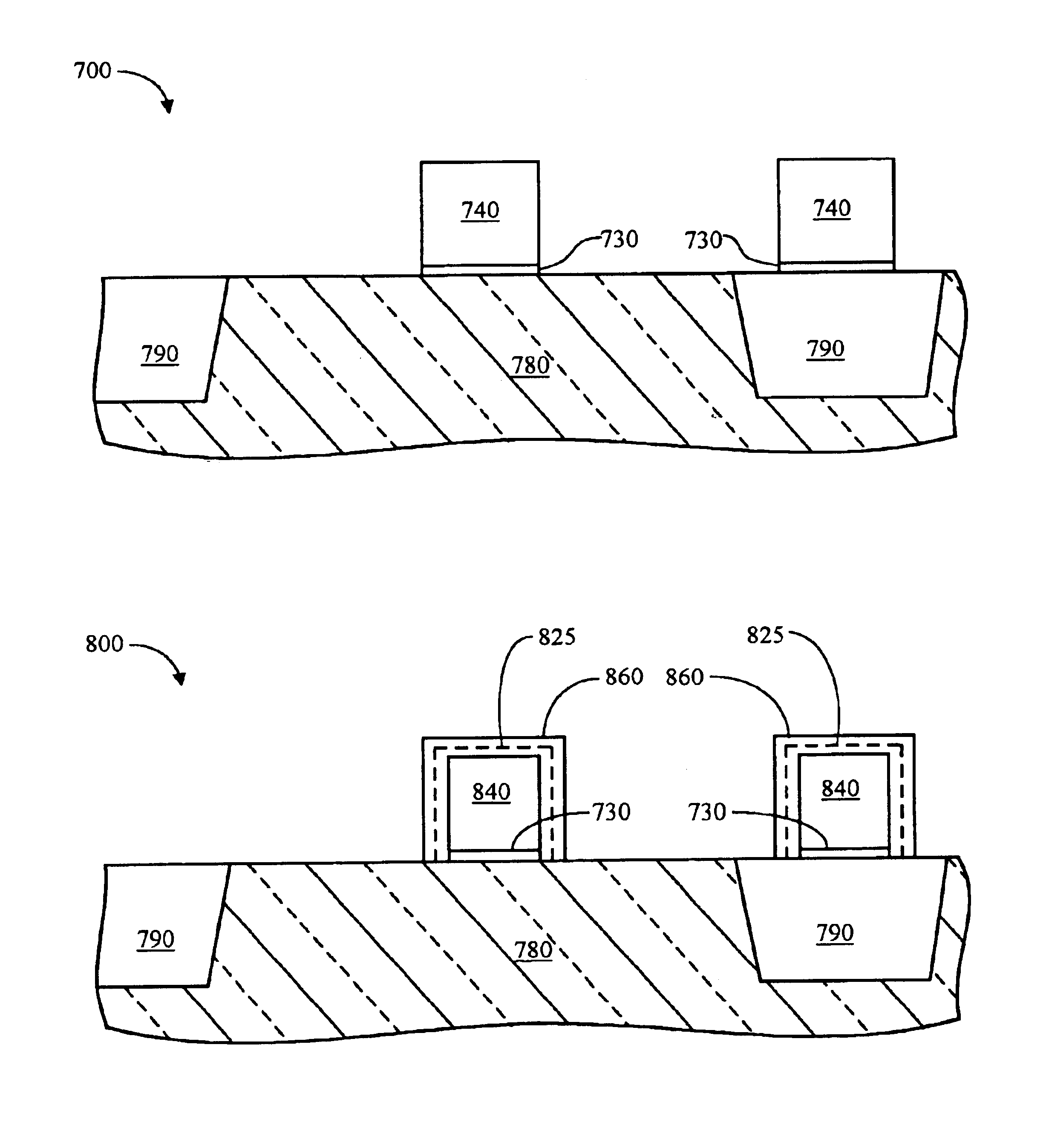
Trimming by Selective Surface Nitridation or Oxidation. In a further embodiment of gate conductor processing by means of laser mediated film growth, one may use these methods to selectively trim the gate conductor line width by means of growing a dielectric film around the entire exposed surface area of the gate conductor. In this application, one generally desires to grow about 10-30 nm of nitride (or oxide), rather than the 50-100 nm of nitride generally described for the borderless contact copending patent application referenced above. As a result, when nitride is grown to trim the gate conductor, milder process conditions are used for ammonia pressure and the number of pulses. When nitride is grown, the energy fluence is maintained at 400-500 mJ / cm.sup.2 per pulse in order to effectively melt the surface of the polysilicon.

A wafer substrate is provided as described in EXAMPLE 1 above, except that the oxide and nitride spacers on the gate conductor are eliminated. In place of the...


PUM


Abstract

A method for forming a trimmed gate in a transistor comprises the steps of forming a polysilicon gate conductor on a semiconductor substrate and trimming the polysilicon portion by a film growth method chosen from among selective surface oxidation and selective surface nitridation. The trimming step may selectively compensate n-channel and p-channel devices. Also, the trimming film may optionally be removed by a method chosen from among anisotropic and isotropic etching. Further, gate conductor spacers may be formed by anisotropic etching of the grown film. The resulting transistor may comprise a trimmed polysilicon portion of a gate conductor, wherein the trimming occurred by a film growth method chosen from among selective surface oxidation and selective surface nitridation.

Description

1. Technical FieldThis invention relates to the field of transistor gate conductor structures in semiconductor devices. More specifically, the invention relates to a method for forming a trimmed gate in a transistor and the apparatus formed thereby.2. Background ArtThe need to remain cost and performance competitive in the production of semiconductor devices has caused continually increasing device density in integrated circuits. To facilitate the increase in device density, new technologies are constantly needed to allow the feature size of these semiconductor devices to be reduced. The push for ever increasing device densities is particularly strong in complimentary metal-oxide semiconductor (CMOS) technologies, such as in the design and fabrication of field effect transistors (FETs). FETs are used in almost all types of integrated circuit design (i.e., microprocessors, memory, etc.)One feature that increases device density is a "trimmed" gate conductor. In general, it is desirabl...

Claims


Application Information

Patent Timeline
Patent Type & Authority Patents(United States)
IPC IPC(8): H01L21/02H01L21/60H01L21/70H01L21/768
CPCH01L21/76888H01L21/76895H01L21/76897
Inventor FURUKAWA, TOSHIHARUHAKEY, MARK C.HOLMES, STEVEN J.HORAK, DAVID V.RABIDOUX, PAUL A.
Owner INT BUSINESS MASCH CORP
Why Eureka
Try Eureka