

Method for forming patterns of a semiconductor device
a technology of semiconductor devices and patterns, applied in the direction of semiconductor devices, photomechanical devices, instruments, etc., can solve the problems of ineffective strategy, inability to develop novel organic anti-reflective films, and collapse of photoresist patterns on top of anti-reflective films, etc., to inhibit the collapse of photoresist patterns and increase the contact area
- Summary
- Abstract
- Description
- Claims
- Application Information
AI Technical Summary
Benefits of technology
Problems solved by technology
Method used
Image

Examples
example 1
Formation of Photoresist Pattern by the Present Invention
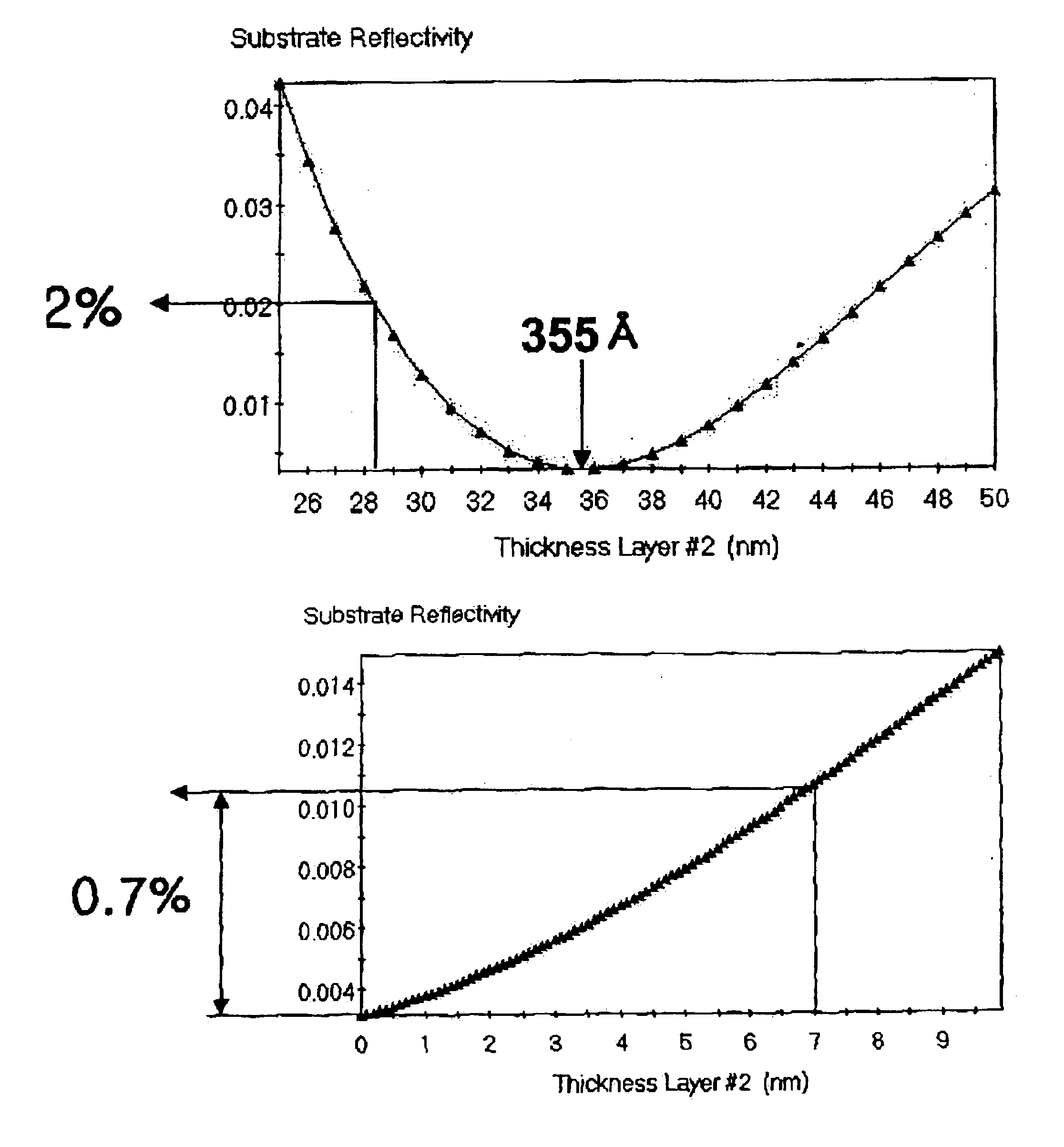
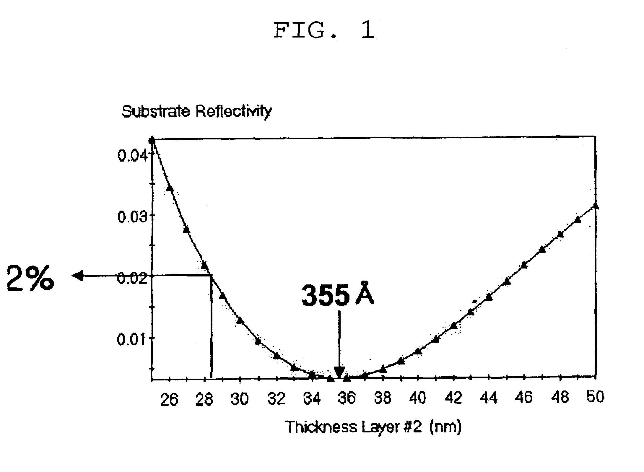
An organic anti-reflective coating composition having a refractive index of 1.64 and light-absorbency of 0.64 at 193 nm light (manufactured by DONG-JIN SEMICHEM corp., which has the trade name of DARC-20 available for a 355 .ANG. coating) was spin-coated on a silicon wafer, baked at 240.degree. C. for 90 seconds to generate cross-linkage bonds and, thereby forming the intended first anti-reflective film with a 355 .ANG. thickness. Again, onto the coated anti-reflective film, another organic anti-reflective coating composition having a refractive index of 1.54 and light-absorbency of 0.38 at 193 nm light which has the trade name of DARC-21, baked at 240.degree. C. for 90 seconds to generate cross-linkage bonds and, thereby forming the second anti-reflective film with a 1000 .ANG. thickness. The obtained second anti-reflective film was subjected to etching process using e-MAX etching apparatus (available from AMAT corp.). Such a...
example 2
Formation of Photoresist Pattern by the Present Invention
An organic anti-reflective coating composition having a refractive index of 1.64 and light-absorbency of 0.64 at 193 nm light (manufactured by DONG-JIN SEMICHEM corp., which has the trade name of DARC-20 available for a 355 .ANG. coating) was spin-coated on a silicon wafer, baked at 240.degree. C. for 90 seconds to generate cross-linkage bonds and, thereby forming the intended first anti-reflective film with a 355 .ANG. thickness. Again, onto the coated anti-reflective film, another organic anti-reflective coating composition having a refractive index of 1.49 and light-absorbency of 0.33 at 193 nm light which has the trade name DARC-21, baked at 240.degree. C. for 90 seconds to generate cross-linkage bonds and, thereby forming the second anti-reflective film with a 1000 .ANG. thickness. The obtained second anti-reflective film was subjected to an etching process using e-MAX etching apparatus (available from AMAT corp.). Such a...
PUM
| Property | Measurement | Unit |
|---|---|---|
| refractive index | aaaaa | aaaaa |
| refractive index | aaaaa | aaaaa |
| refractive index | aaaaa | aaaaa |
Abstract
Description
Claims
Application Information