Display panel and display device to which the display panel is applied

a display panel and display device technology, applied in the field of display panel and display device to which the display is applied, can solve the problems of affecting the performance of the display panel, the effect of reducing the fluorescence layer caused by the charge cannot be prevented, and the image quality is highly likely to be affected

Inactive Publication Date: 2004-08-03
SONY CORP
View PDF9 Cites 49 Cited by
  • Summary
  • Abstract
  • Description
  • Claims
  • Application Information

AI Technical Summary

Benefits of technology

It is therefore a first object of the present invention to provide a display panel in which the deterioration of its fluorescence layer caused by a charge can be prevented, and a display device having a long lifetime due to the use of the above display panel.
In the display device according to each of the first to third aspects of the present invention, a cold cathode field emission device (to be referred to as "field emission device" hereinafter) is preferred as an electron emitting member. The type of the field emission device is not specially limited, and it can be any one of a Spindt type field emission device, an edge type field emission device, a flat type field emission device, a low-profile type field emission device and a crown type field emission device. Generally, the electron emitting member(s) is arranged in a region where each of projection images of a first electrode group extending in one direction in which scanning signals are inputted and a second electrode group extending in the other direction in which video signals are inputted overlaps each other. In the display device according to each of the second and third aspects of the present invention, preferably, the independent electrodes are arranged in the form of stripes and extend in a direction nearly in parallel with the direction of the second electrode group for achieving the third object of the present invention to prevent a variability of brightness in a display screen caused depending upon the number of selected electrodes of the second electrode group. When the first electrode group comprises gate electrodes, the second electrode group comprises cathode electrodes. When the first electrode group comprises cathode electrodes, the second electrode group comprises gate electrodes.

Problems solved by technology

Meanwhile, an FED which is a flat type display device has a far smaller flying distance of electrons than a cathode ray tube, so that the electron acceleration voltage cannot be so increased as a cathode ray tube.
That is, when the electron acceleration voltage is too high in the FED, a spark discharge is liable to take place very easily between the electron emitting portion on the rear panel and the film which works as an anode electrode, which may highly possibly downgrade the image quality to a large extent.
In a general production process of display panels or display devices using the display panels, practicing the above control involves great technical difficulties.
The FED for which a low acceleration voltage of electrons is inevitably selected causes characteristic problems which are not found in a cathode ray tube.
The above degradation of the fluorescence layer leads to a variance in the color of emitted light or light emission efficiency and contamination of components inside the FED and finally to a decrease in the reliability and lifetime characteristic of the FED.
Further, the conventional FED has another problem that the brightness of a display screen varies depending upon pixels or sub-pixels selected on the rear panel 400 side. FIGS. 27A and 27B show schematic configurations of the real panel 400.

Method used


Image

  • Display panel and display device to which the display panel is applied
  • Display panel and display device to which the display panel is applied
  • Display panel and display device to which the display panel is applied

Examples


example 1

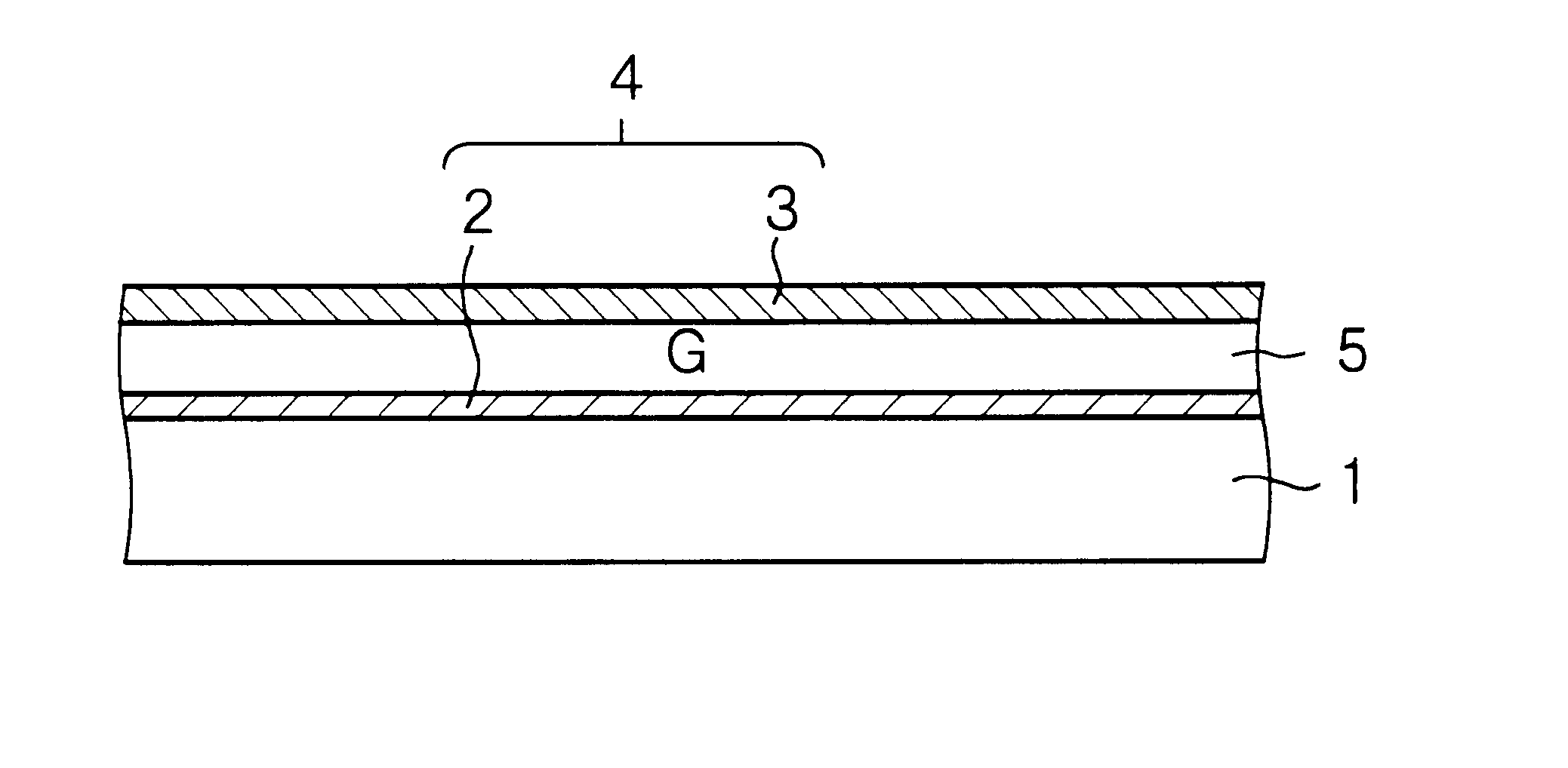
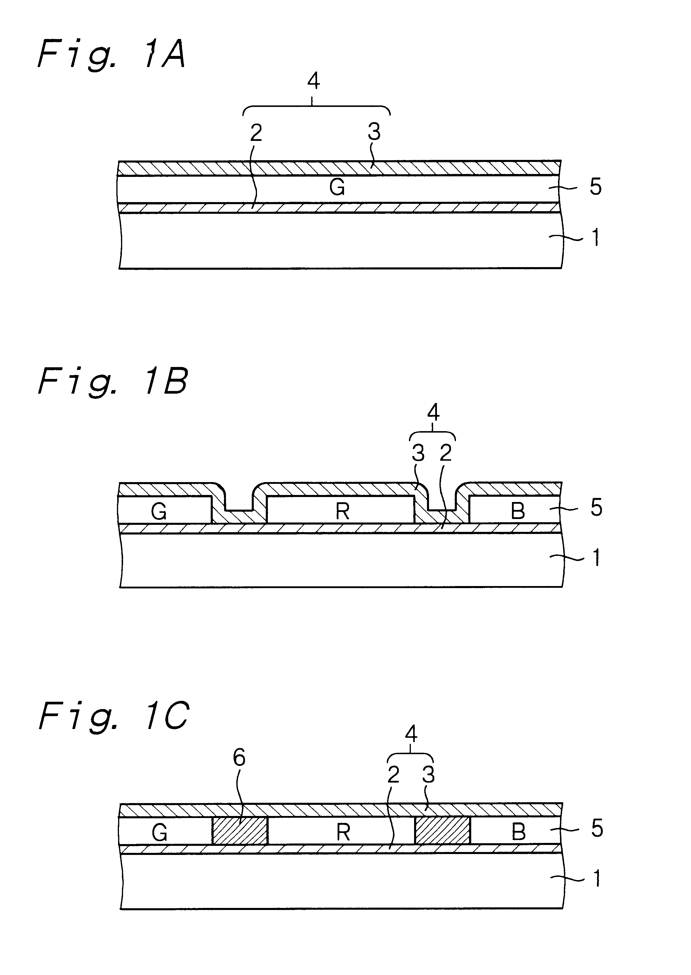
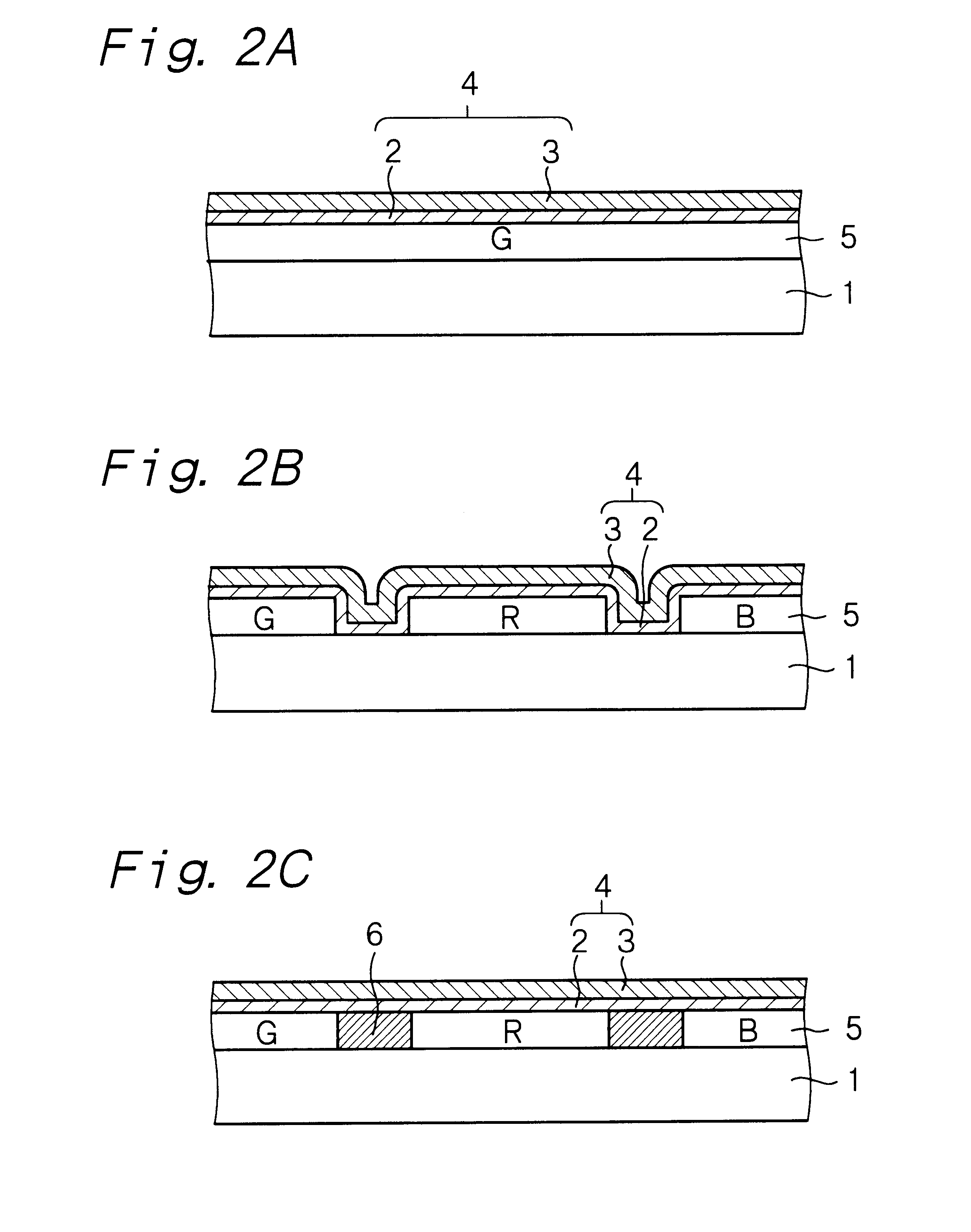
is concerned with a display panel and a display device according to the first aspect of the present invention. FIGS. 1A to 1C show schematic partial cross-sectional views of the display panels of the case (i), FIGS. 2A to 2C show schematic partial cross-sectional views of the display panels of the case (ii), FIG. 3 shows a conceptual view of the display device, and FIGS. 4A and 4B show brightness lifetime characteristics of the display devices.

FIGS. 1A to 1C show configuration examples of three types of the display panels belonging to the case (i). An anode electrode 4 comprises a lower electrode 2 and an upper electrode 3, the lower electrode 2 is formed on a substrate 1, a fluorescence layer 5 is formed on the lower electrode 2, and the upper electrode 3 is formed on the fluorescence layer 5. The display panel shown in FIG. 1A is intended to be a display panel for monochromatic displaying, and the fluorescence layer for emitting light, for example, of green (G) is formed on the en...

example 2

Example 2 is concerned with a display panel according to the second-C constitution and a display device according to the second aspect of the present invention. FIG. 5A is a schematic partial plan view and FIGS. 5B to 5E and FIGS. 6A to 6D are schematic partial cross-sectional views of the display panels of Example 2. FIG. 7 shows a conceptual view of the display device. FIGS. 8A to 8C, FIGS. 9A to 9D, FIGS. 10A to 10E and FIGS. 11A to 11D show patterns of combinations of an independent electrode and a substrate.

In a display panel 100 of Example 2, an anode electrode comprises a plurality of independent electrodes 13 so formed as to correspond to a predetermined number of unit fluorescence layers as shown in FIG. 5A. A plurality of these independent electrodes 13 are arranged as a whole to nearly cover the effective region. A power supply line is formed on a rectangular substrate 10 composed, for example, of glass, and the power supply line comprises one main line 14 extending in th...

example 3

Example 3 is concerned with a display panel as other examples of the display panel of the second-C constitution, in which the independent electrodes are formed such that one independent electrode corresponds to one unit fluorescence layer. FIG. 12A shows a schematic plan view of the display panel of Example 3. As shown in FIG. 12A, the anode electrode of the display panel 101 comprises a plurality of independent electrodes 113 which are formed in the form of a matrix such that the independent electrodes are so formed as to correspond to the unit fluorescence layers 112R, 112G, . . . respectively. A plurality of these independent electrodes 113 as a whole are arranged to nearly cover the effective region. The power supply line is formed on the rectangular substrate 110 composed, for example, of glass, and it comprises one main line 114 extending in the width direction of the rectangular substrate 110 and a plurality of branch lines 124 extending from the main line 114 and in the colu...


PUM


Abstract

A display panel comprising a substrate, a fluorescence layer which is to be caused to emit light by electrons from a vacuum space, and an anode electrode which is to direct the electrons toward the fluorescence layer, wherein the anode electrode comprises a lower electrode and an upper electrode.

Description

BACKGROUND OF THE INVENTION AND RELATED ART STATEMENTThe present invention relates to a display panel and a display device to which the display panel is applied. More specifically, it relates to a display panel having a fluorescence layer which is excited by electrons from a vacuum space to emit light, and a display device into which the display panel is incorporated.Various flat type (flat panel type) displays are being studied as image display devices which are to replace currently main-stream cathode ray tubes (CRT). The flat type displays include a liquid crystal display (LCD), an electroluminescence display device (ELD) and a plasma display panel (PDP). Further, there is also proposed a cold cathode field emission display device, a so-called field emission device (FED), which is capable of emitting electrons into vacuum from a solid without relying on thermal excitation, and it attracts attention from the viewpoint of a brightness on a screen and a low power consumption.FIG. 24...

Claims


Application Information

Patent Timeline
Patent Type & Authority Patents(United States)
IPC IPC(8): G09G3/30H01J29/08H01J31/12
CPCH01J29/085H01J31/127
Inventor KONISHI, MORIKAZUOKITA, MASAMIIGARASHI, TAKAHIROKUSUNOKI, TSUNEOOHNO, KATSUTOSHI
Owner SONY CORP
Why Eureka
Try Eureka