Method and apparatus for identifying misregistration in a complimentary phase shift mask process

a phase shift mask and misregistration technology, applied in the field of semiconductor device manufacturing, can solve the problems of engendering nonoptimal control of critical processing parameters, many of the processing tools currently commercially available suffer certain deficiencies, and tools often lack advanced process data monitoring capabilities

Inactive Publication Date: 2004-08-10
GLOBALFOUNDRIES US INC
View PDF6 Cites 58 Cited by
  • Summary
  • Abstract
  • Description
  • Claims
  • Application Information

AI Technical Summary

Problems solved by technology

However, despite the advances made in this area, many of the processing tools that are currently commercially available suffer certain deficiencies.
In particular, such tools often lack advanced process data monitoring capabilities, such as the ability to provide historical parametric data in a user-friendly format, as well as event logging, real-time graphical display of both current processing parameters and the processing parameters of the entire run, and remote, i.e., local site and worldwide, monitoring.
These deficiencies can engender nonoptimal control of critical processing parameters, such as throughput, accuracy, stability and repeatability, processing temperatures, mechanical tool parameters, and the like.
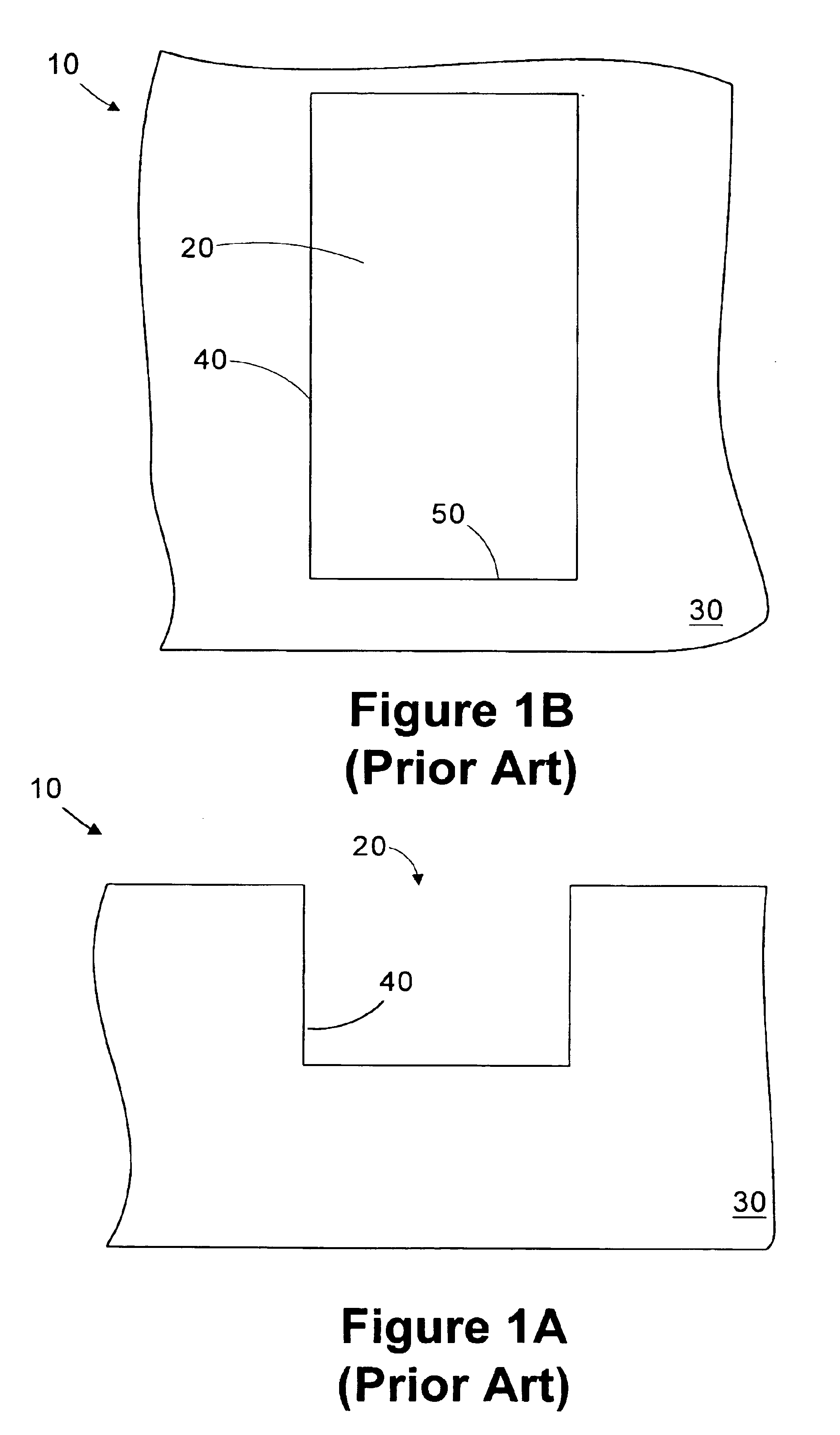
Due to limitations imposed by the wavelength of light used to transfer the pattern, resolution at the edges of the patterns of the photomask degrades, thus limiting the application of the binary mask as the geometry of the features to be formed on the wafer decreases.
In some instances, these nulls may form in regions where it is not desirable to form a feature in the underlying photoresist layer.
If a misalignment occurs between the two masks, the binary mask may not erase all of the artifacts formed by the phase shift mask patterning process.

Method used


Image

  • Method and apparatus for identifying misregistration in a complimentary phase shift mask process
  • Method and apparatus for identifying misregistration in a complimentary phase shift mask process
  • Method and apparatus for identifying misregistration in a complimentary phase shift mask process

Examples


Embodiment Construction

Illustrative embodiments of the invention are described below. In the interest of clarity, not all features of an actual implementation are described in this specification. It will of course be appreciated that in the development of any such actual embodiment, numerous implementation-specific decisions must be made to achieve the developers' specific goals, such as compliance with system-related and business-related constraints, which will vary from one implementation to another. Moreover, it will be appreciated that such a development effort might be complex and time-consuming, but would nevertheless be a routine undertaking for those of ordinary skill in the art having the benefit of this disclosure.

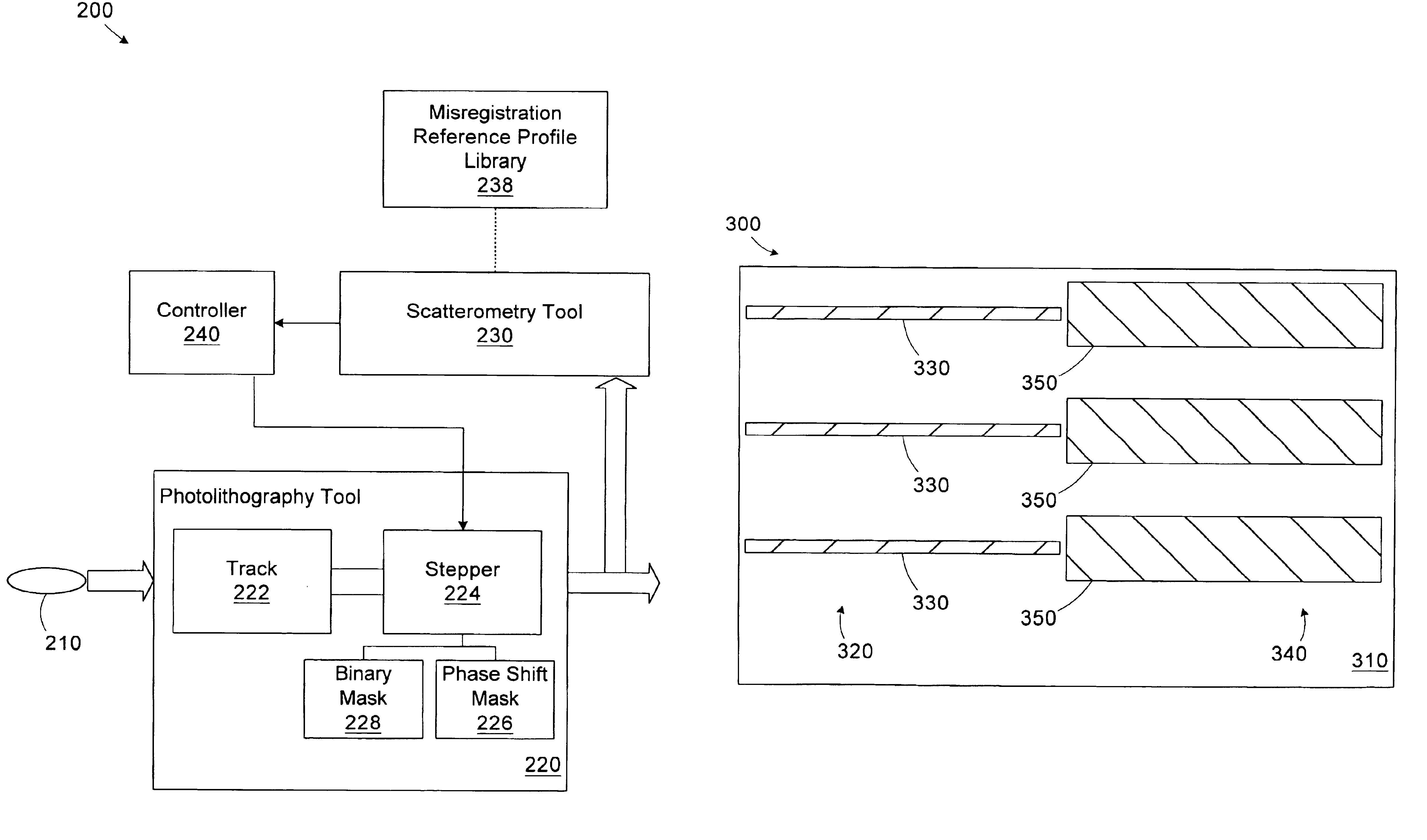
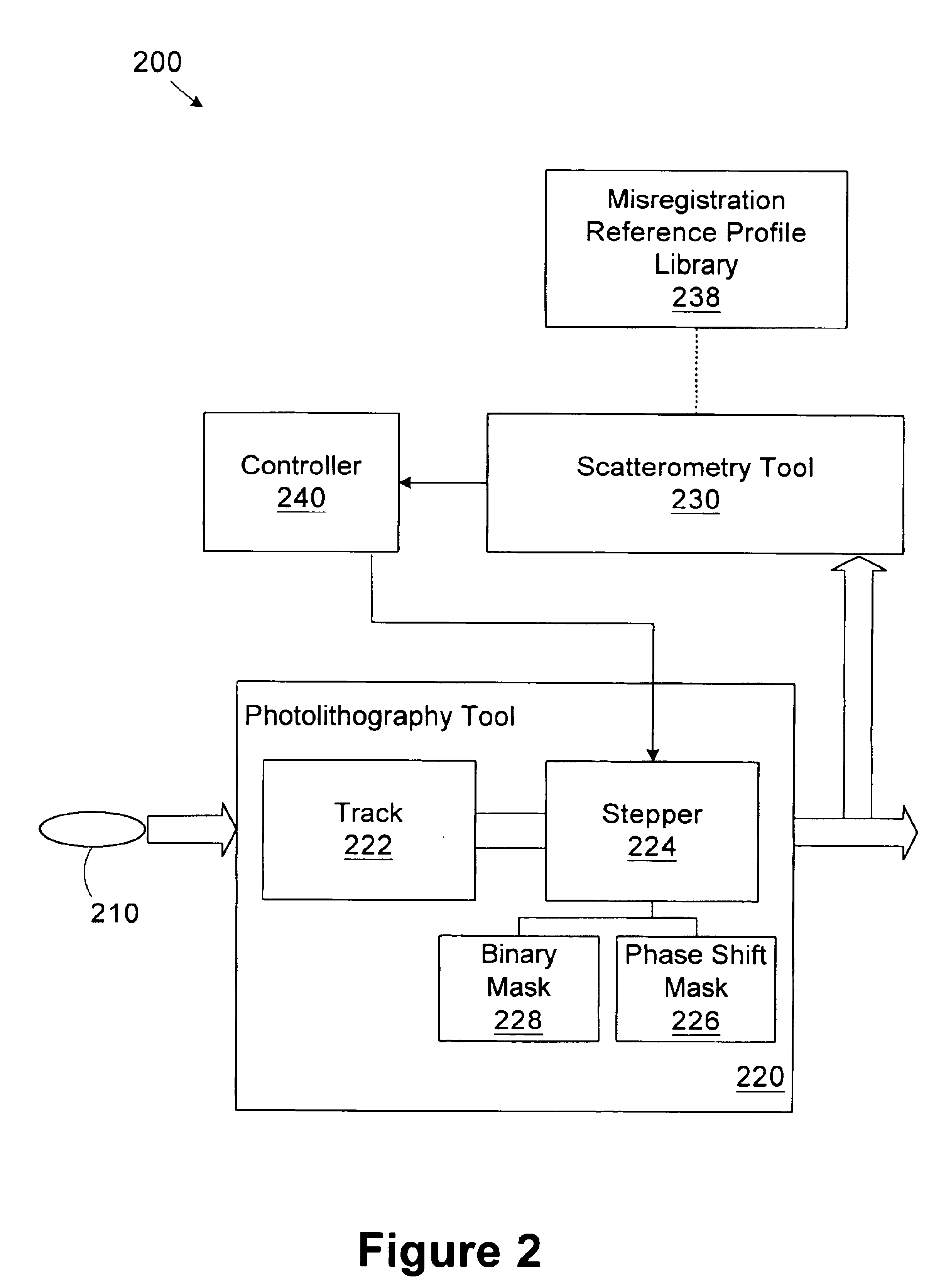
Referring to FIG. 2, a simplified diagram of an illustrative processing line 200 for processing wafers 210 in accordance with one illustrative embodiment of the present invention is provided. The processing line 200 includes a photolithography tool 220 for forming a pattern in a photor...


PUM

PropertyMeasurementUnit
widthaaaaaaaaaa
widthaaaaaaaaaa
widthaaaaaaaaaa

Abstract

A method includes providing a wafer having a first grating structure and a second grating structure formed in a photoresist layer. At least a portion of the first and second grating structures is illuminated with a light source. Light reflected from the illuminated portion of the first and second grating structures is measured to generate a reflection profile. Misregistration between the first and second grating structures is determined based on the reflection profile. A processing line includes a photolithography stepper, a metrology tool, and a controller. The photolithography stepper is adapted to process wafers in accordance with an operating recipe. The metrology tool is adapted to receive a wafer processed in the stepper. The wafer has a first grating structure and a second grating structure formed in a photoresist layer. The metrology tool includes a light source, a detector, and a data processing unit.

Description

1. Field of the InventionThis invention relates generally to the field of semiconductor device manufacturing and, more particularly, to a method and apparatus for identifying misregistration in a complimentary phase shift mask process.2. Description of the Related ArtThere is a constant drive within the semiconductor industry to increase the quality, reliability and throughput of integrated circuit devices, e.g., microprocessors, memory devices, and the like. This drive is fueled by consumer demands for higher quality computers and electronic devices that operate more reliably. These demands have resulted in a continual improvement in the manufacture of semiconductor devices, e.g., transistors, as well as in the manufacture of integrated circuit devices incorporating such transistors. Additionally, reducing the defects in the manufacture of the components of a typical transistor also lowers the overall cost per transistor as well as the cost of integrated circuit devices incorporati...

Claims


Application Information

Patent Timeline
Patent Type & Authority Patents(United States)
IPC IPC(8): G03F7/20
CPCG03F7/70633
Inventor WRIGHT, MARILYN I.LENSING, KEVIN R.STIRTON, JAMES BROC
Owner GLOBALFOUNDRIES US INC
Why Eureka
Try Eureka