Glass ceramic multilayer substrate manufacturing method and glass ceramic multilayer substrate product

a glass ceramic and multi-layer substrate technology, applied in the direction of electrical equipment, basic electric elements, solid-state devices, etc., can solve the problems of changing the shrinking behavior of glass material surrounding the wiring conductor, difficult to produce a glass ceramic multi-layer substrate which is completely flat, and the shrinkage of one glass ceramic multi-layer substrate will not always be the sam

Inactive Publication Date: 2004-09-28
MURATA MFG CO LTD
View PDF18 Cites 20 Cited by
  • Summary
  • Abstract
  • Description
  • Claims
  • Application Information

AI Technical Summary

Benefits of technology

The glass ceramic multilayer substrate manufacturing method according to the present invention comprises a step (hereinafter sometimes referred to as a first step) of preparing first green sheets each containing as its solid components, a first glass powder and a first ceramic powder; a step (hereinafter sometimes referred to as a second step) of preparing second green sheets each containing as its solid components, a second glass powder and a second ceramic powder and capable of exhibiting a sintering shrinkage different from that of the first green sheets; a step (hereinafter sometimes referred to as a third step) of forming conductor films and / or via-hole conductors in the first green sheets and / or the second green sheets; a step (hereinafter sometimes referred to as a fourth step) of forming an unsintered laminated body by laminating together at least one of the first green sheets and at least one of the second green sheets; and a step (hereinafter sometimes referred to as a fifth step) of sintering the laminated body. The method is characterized by the following aspects which are effective for solving the aforementioned problems peculiar to the above-described conventional methods.

Problems solved by technology

However, the aforementioned sintering treatment has encountered the following problems.
Further, metal components contained in the electrically conductive paste will be dispersed into the glass material contained in the green sheets, and this will cause a change in the shrinking behavior of the glass material surrounding the wiring conductors.
As a result, it is difficult to produce a glass ceramic multilayer substrate which is completely flat without any warpage.
Moreover, the sintering shrinkage of one glass ceramic multilayer substrate will not always be the same as that of another.
As a result, the attachment size error will often go beyond an allowable range in a process where electronic parts are attached to a substrate in a manner as if flip chips are attached thereto, thus rendering it extremely difficult to ensure a high yield in an industrial production.
However, the arresting green sheet(s) formed on one or both sides of the unsintered laminated body in the above-described method will have to be removed after the sintering process is over.
Because of this, the total cost for manufacturing a glass ceramic multilayer substrate is high, since the entire manufacturing cost will include a cost for forming the arresting green sheet(s) and also a cost for removing the arresting green sheet(s).
However, the glass ceramic multilayer substrate manufacturing method disclosed in Japanese Unexamined Patent Application Publication Nos. 6-97656 and 6-172017 also has a problem that in carrying out the process disclosed in these patent publications, it will sometimes be difficult to sufficiently inhibit shrinkage in the plane direction of a laminated body during the sintering process, and it will also be occasionally difficult to ensure that a sintering shrinkage can be controlled within 10%.
It is difficult to exactly produce an improved glass ceramic multilayer substrate having a sufficient flatness.
The above troubles are associated with the difference between a shrinkage ending temperature of one group of green sheets and the shrinkage starting temperature of the other group of green sheets, and also related to a temperature rising speed in the sintering process.
Further, it has been found that the above troubles happen early if there is only a small difference between the shrinkage ending temperature of one group of green sheets and the shrinkage starting temperature of the other group of green sheets, and also if the temperature rising speed is high in the sintering process.
However, this will require a longer operation time for completing the sintering treatment and thus not advisable in view of a increased costs.
In fact, such kind of small cracks will remarkably reduce the strength of thus produced glass ceramic multilayer substrate.

Method used


Image

  • Glass ceramic multilayer substrate manufacturing method and glass ceramic multilayer substrate product
  • Glass ceramic multilayer substrate manufacturing method and glass ceramic multilayer substrate product
  • Glass ceramic multilayer substrate manufacturing method and glass ceramic multilayer substrate product

Examples


Embodiment Construction

In the following, the present invention will be described by giving an example.

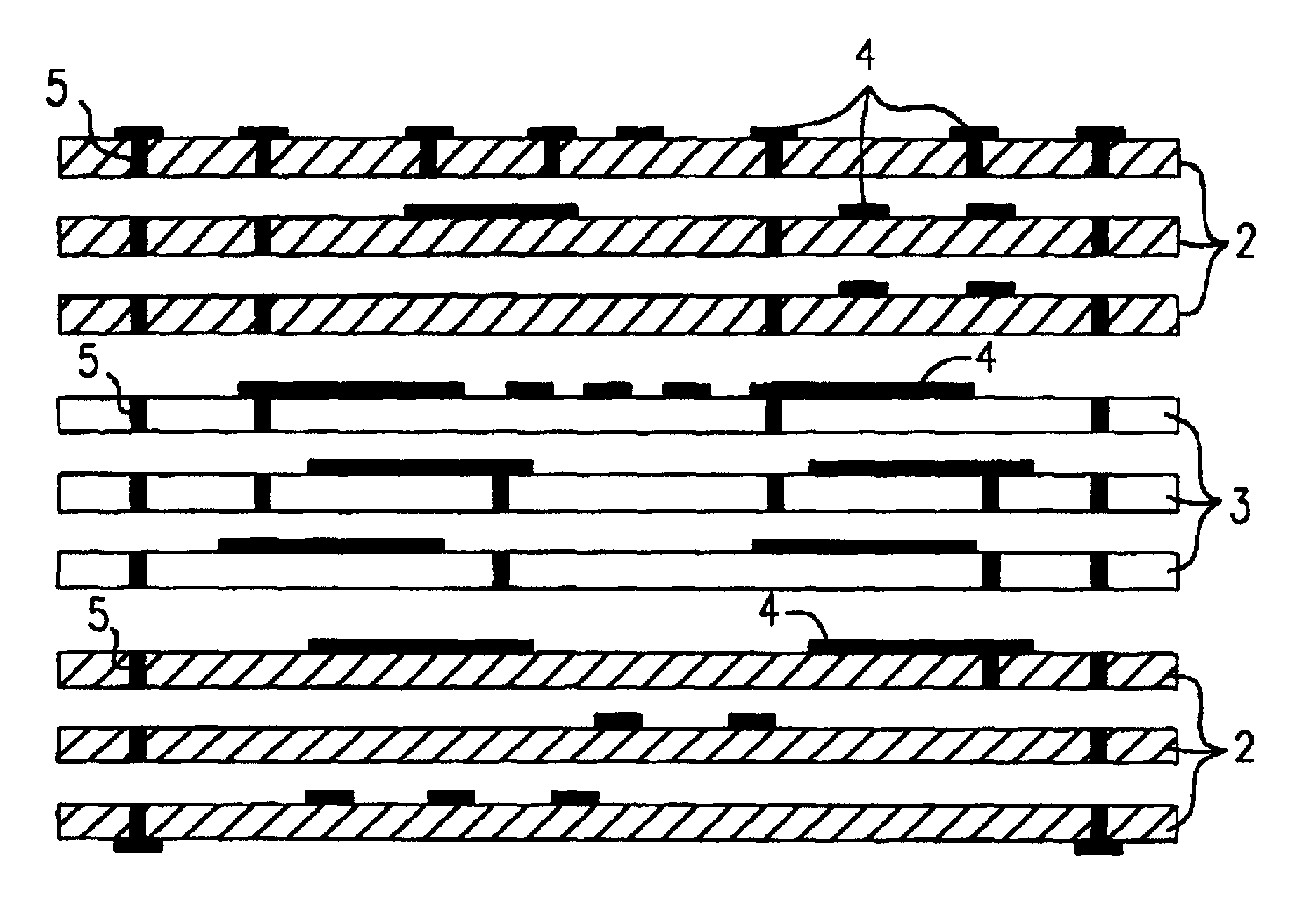
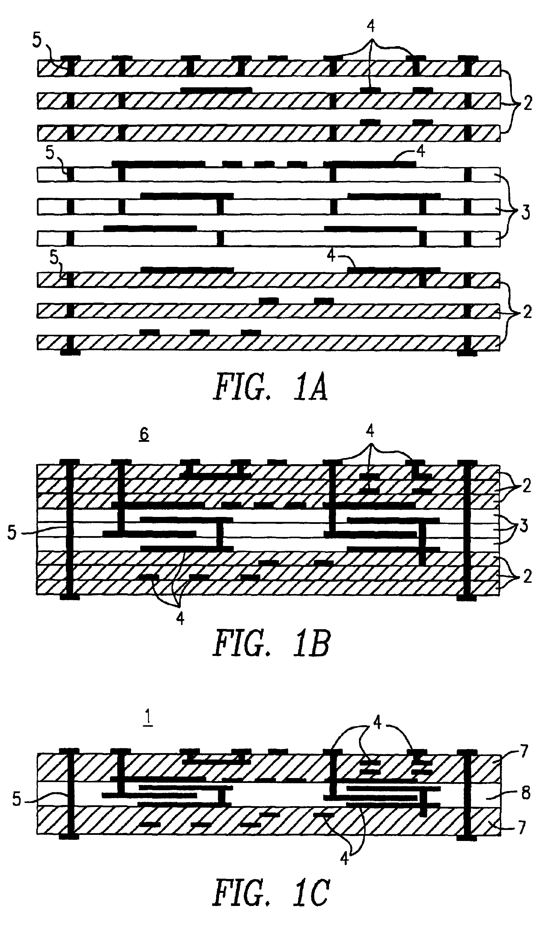
BaO--MgO--SiO.sub.2 --B.sub.2 --O.sub.3 glass powder and alumina powder were mixed together using a mixing ratio of 80:20, thereby forming a powder mixture. Then, an acryl resin, a xylene resin, butanol, a plasticizer and a dispersing agent were mixed into the powder mixture, thereby forming a slurry. Subsequently, the doctor blade method was used to prepare first green sheets 2 shown in FIG. 1A.

MgO--ZnO--SiO.sub.2 --B.sub.2 O.sub.3 glass powder and BaO--Sm.sub.2 O.sub.3 --SiO.sub.2 --TiO.sub.2 ceramic powder were mixed together using a mixing ratio of 30:70, thereby forming a powder mixture. Then, second green sheets 3 shown in FIG. 1A were obtained in the same method as used for preparing the first green sheets 2.

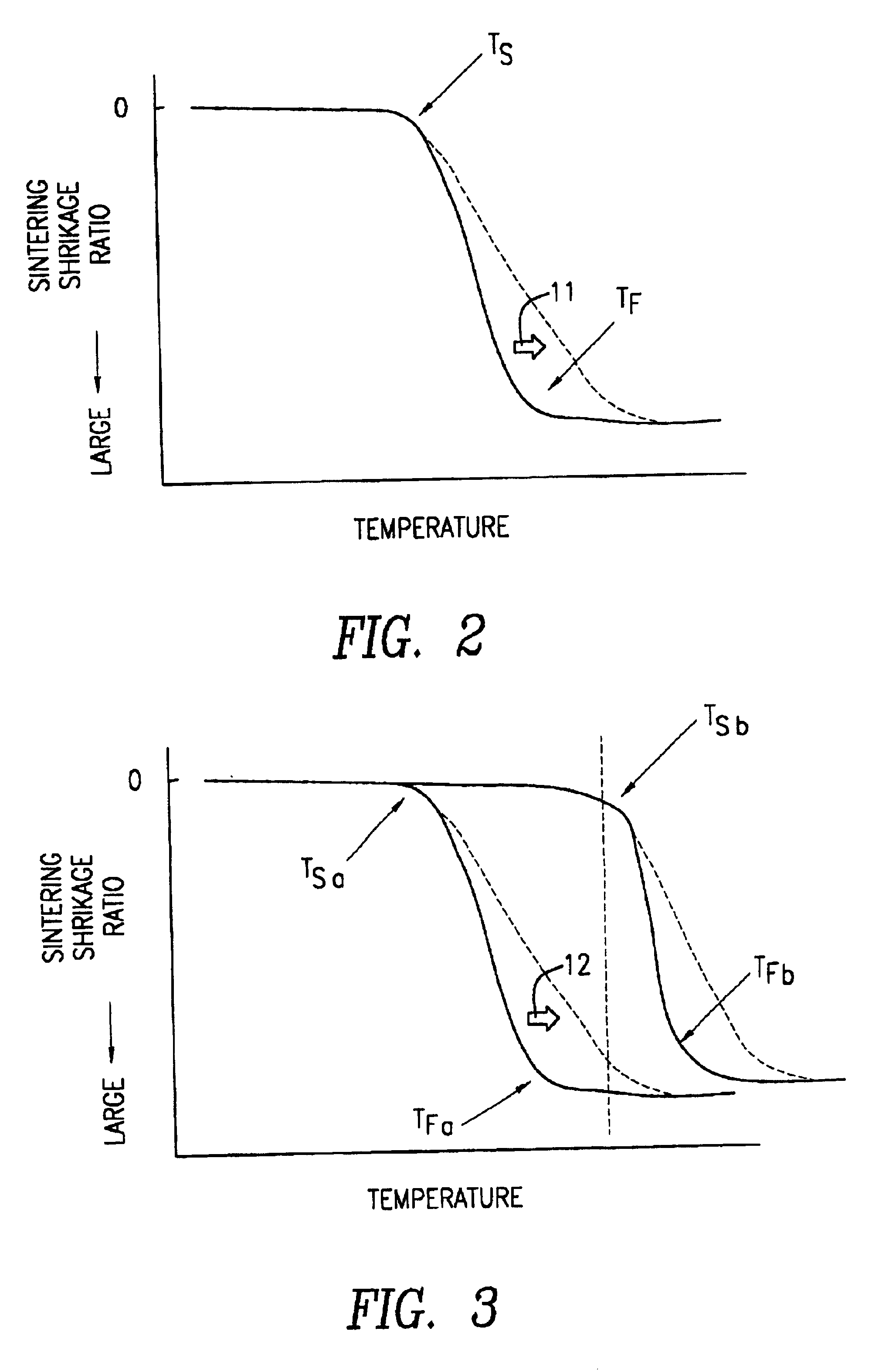
The first and second green sheets 2 and 3 were measured to detect their shrinkage starting temperatures TSa and TSb and sintering process ending temperatures TFa and TFb (when a shrinkage is 90...


PUM

PropertyMeasurementUnit
shrinkageaaaaaaaaaa
glass transition temperatureaaaaaaaaaa
shrinkage ratioaaaaaaaaaa

Abstract

A glass ceramic multilayer substrate having a better flatness and a low sintering shrinkage ratio is made by sintering an unsintered laminated body formed by laminating together first and second green sheets capable of exhibiting different shrinking behaviors during a sintering process, thereby producing the desired glass ceramic multilayer substrate. When the shrinkage starting temperatures (°C.) of the first and second green sheets are TSa and TSb, the sintering process ending temperatures (°C.) of the first and second green sheets are TFa and TFb, and when the temperature rising speed is X° C. / min, the respective parameters satisfy (TFa+3X)<TSb or (TFb+3X)<TSA.

Description

1. Field of the InventionThe present invention relates to a method for manufacturing a glass ceramic multilayer substrate, and also relates to a glass ceramic multilayer substrate product obtained by using the manufacturing method. In detail, this invention relates to an improvement which can more reliably inhibit the undesired shrinkage that occurs in a sintering process for obtaining a glass ceramic multilayer substrate.2. Description of the Related ArtWhen manufacturing a ceramic multilayer substrate having wiring conductors such as conductor film and via-hole conductor, the wiring conductors have to be subjected to sintering during the obtaining of the multilayer substrate. Accordingly, when a low resistance conductor such as Ag and Cu is used to form wiring conductors, the ceramic multilayer substrate has to be made of a material which can be sintered at a temperature equal to or lower than the melting point of Ag, Cu and the like. In order to meet such a requirement, a glass c...

Claims


Application Information

Patent Timeline
Patent Type & Authority Patents(United States)
IPC IPC(8): C04B35/462H01L21/02H01L23/12H01L21/48H01L23/15H05K3/46H05K1/16H05K1/03C03C14/00
CPCB32B18/00C03C14/004C04B35/462H01L21/4867H01L23/15H05K3/4629H05K3/4688C03C14/00Y10T428/24926C03C2214/00C03C2214/20C03C2214/30C04B2235/3206C04B2235/3215C04B2235/3217C04B2235/3222C04B2235/3224C04B2235/3232C04B2235/3244C04B2235/3281C04B2235/3284C04B2235/3409C04B2235/3418C04B2235/36C04B2235/6562C04B2235/9615H01L2924/09701H05K1/0306H05K1/162C04B2237/343C04B2237/348H01L2924/0002H01L2924/00
Inventor MORIYA, YOICHISUGIMOTO, YASUTAKACHIKAGAWA, OSAMU
Owner MURATA MFG CO LTD
Why Eureka
Try Eureka