High frequency circuit chip and method of producing the same

a high-frequency circuit chip and high-frequency technology, applied in the field of circuit chips, can solve the problems of deteriorating the electrical characteristics of such chips, affecting the production efficiency of high-frequency circuit chips, and high cost of reactive ion etching and ion milling apparatuses, etc., to achieve the effect of reducing size, high-precision wiring pattern and efficient production of the sam

Inactive Publication Date: 2005-01-04
MURATA MFG CO LTD
View PDF4 Cites 70 Cited by
  • Summary
  • Abstract
  • Description
  • Claims
  • Application Information

AI Technical Summary

Benefits of technology

In order to overcome the above-described problems, preferred embodiments of the present invention provide a high frequency ci

Problems solved by technology

However, the apparatuses required for reactive ion etching and ion milling are expensive and, moreover, the substrates are chemically damaged, which deteriorates the electrical characteristics of such chips.
7), a resist cannot be uniformly coated, which makes it difficult to form a fine wiring pattern.
Moreover, in high frequency circui

Method used


Image

  • High frequency circuit chip and method of producing the same
  • High frequency circuit chip and method of producing the same
  • High frequency circuit chip and method of producing the same

Examples


Embodiment Construction

Hereinafter, the features of the present invention will be described with reference to preferred embodiments of the present invention.

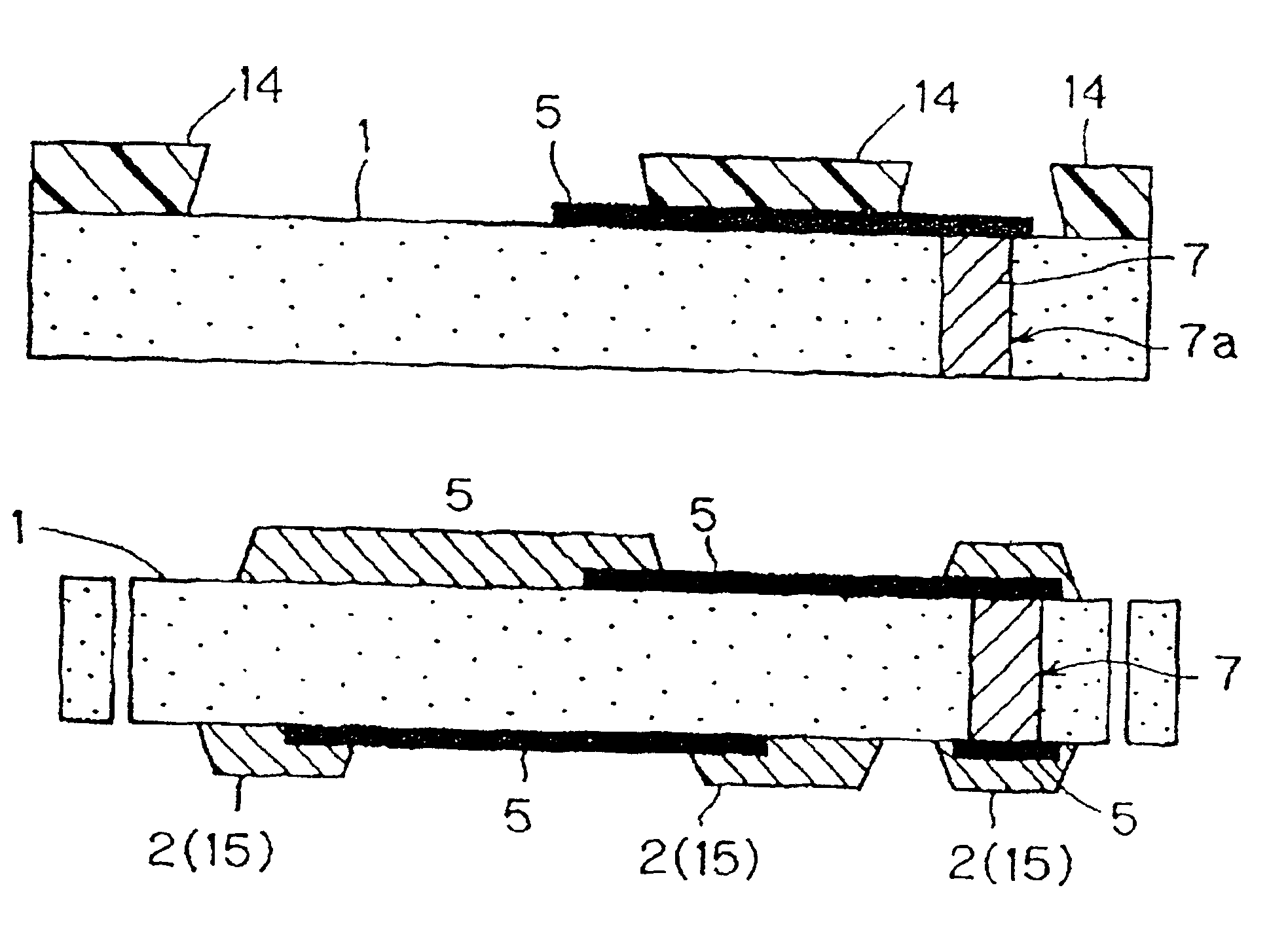
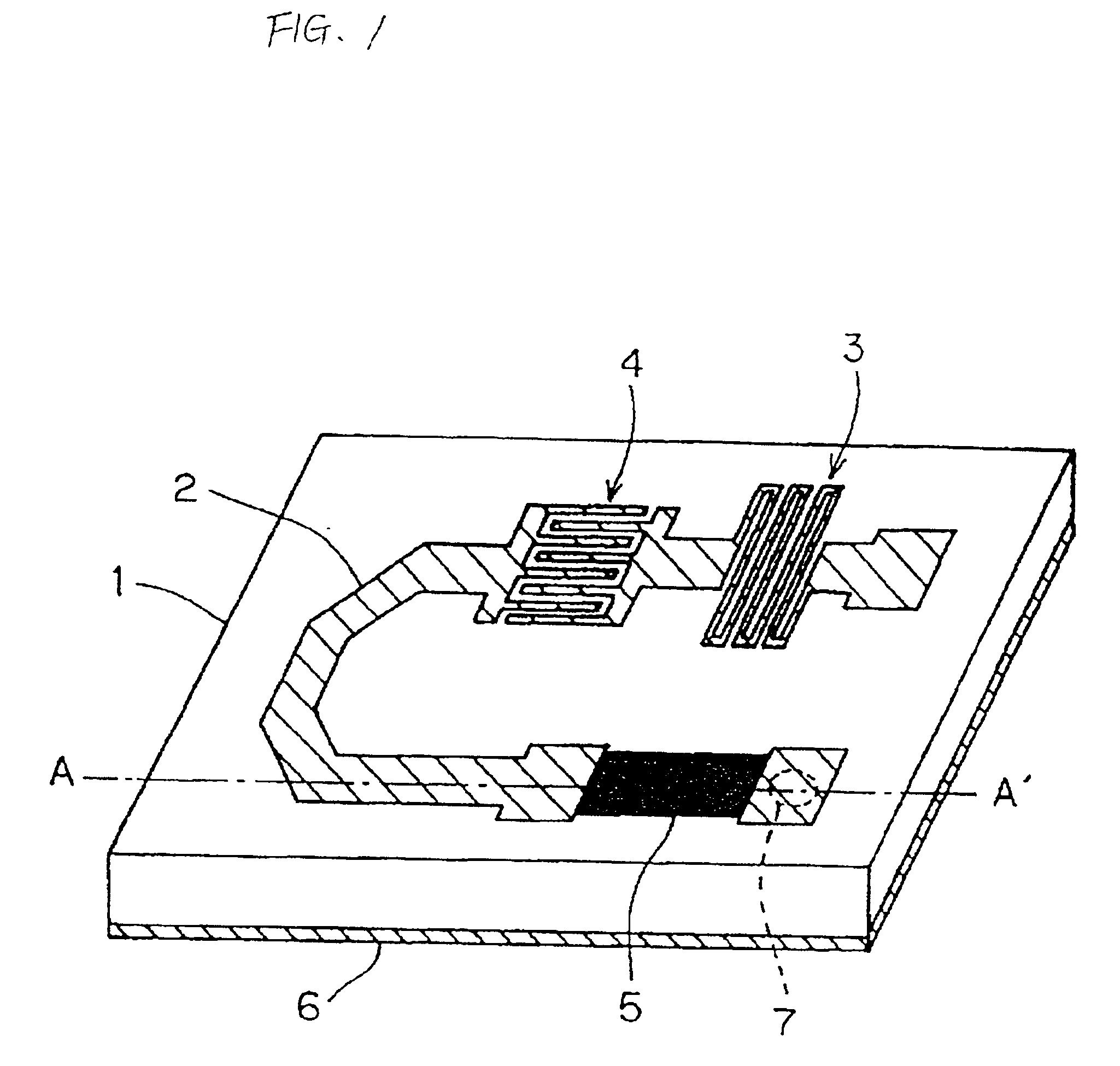
FIG. 1 shows a high frequency circuit chip according to a first preferred embodiment of the present invention. The high frequency circuit chip includes a wiring pattern (e.g., a distributed constant line or a microstrip line) 2 provided on the upper surface (front surface) of a substrate 1, lumped constant elements such as a meander-shaped inductor 3, an interdigital capacitor 4, a thin film resistor 5, and other suitable elements, and a through-hole 7 which connects the wiring pattern 2 provided on the front surface of the substrate 1 and a back-surface electrode (conductor layer) 6 provided on the back surface of the substrate 1 to each other.

Hereinafter, a method of producing a high frequency circuit chip according to the first preferred embodiment of the present invention will be described.

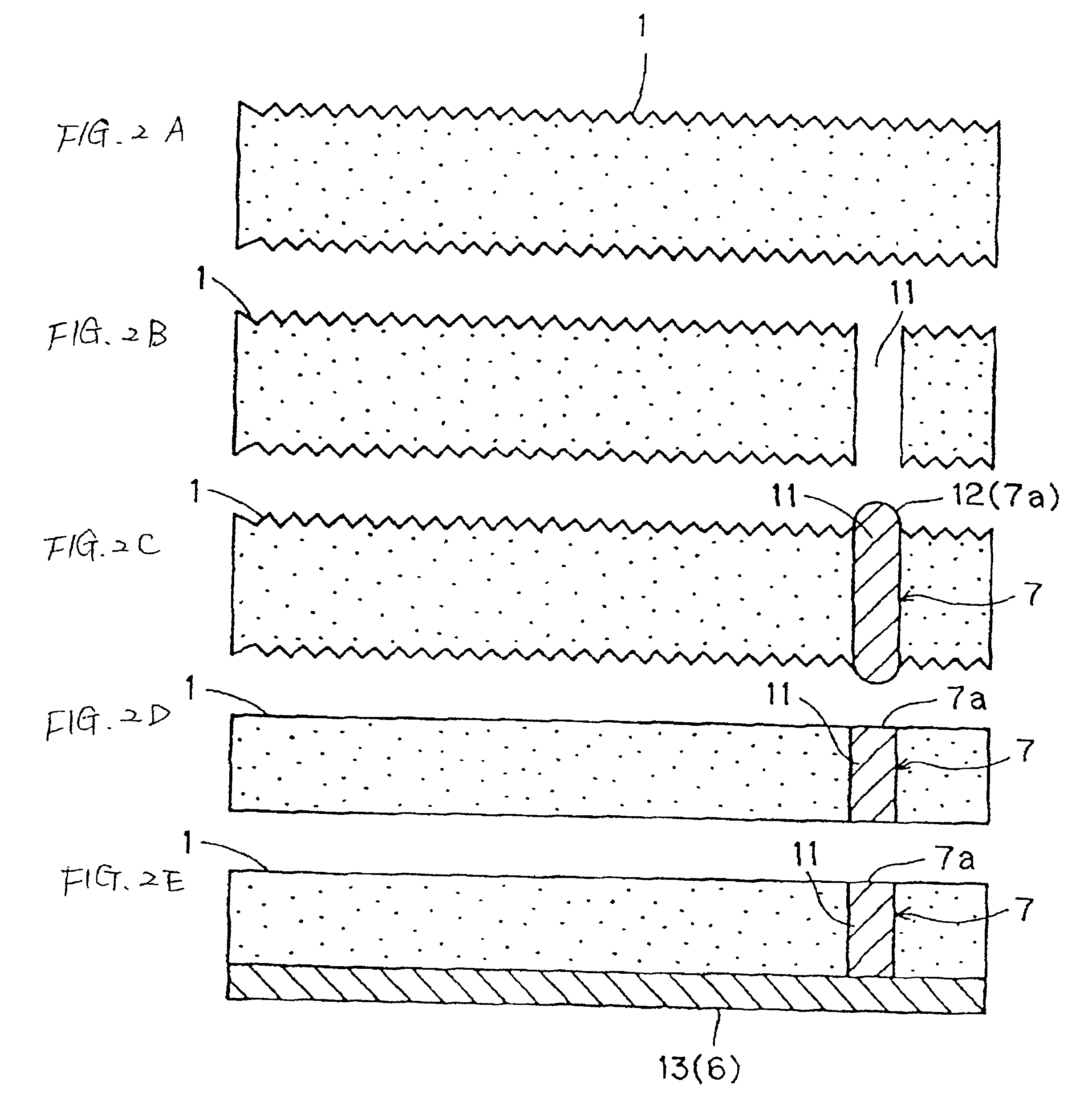
(1) First, a perforation 11 (FIG. 2B) for a through-hole i...


PUM


Abstract

In the production of a high frequency circuit chip in which a wiring pattern is disposed on a substrate having a through-hole, a connecting electrode of the through-hole is formed by filling electrically conductive paste into a perforation and firing it, and the wiring pattern is formed by a lift-off method. Moreover, at least the surface of the substrate for the wiring pattern to be formed thereon is mirror-polished, and thereafter, the wiring pattern is formed on the mirror-polished surface by the lift-off method.

Description

BACKGROUND OF THE INVENTION1. Field of the InventionThe present invention relates to a circuit chip, and, more particularly, to a high frequency circuit chip used in a multi-chip module (MCM) which operates in the microwave and millimeter wave bands, and a method of producing such a high frequency circuit chip.2. Description of the Related ArtAn example of a conventional high frequency circuit chip (passive circuit chip) used in multi-chip modules (MCM) which operate in the microwave and millimeter wave bands, is shown in FIG. 6.The high frequency circuit chip includes lumped constant elements such as a wiring pattern 52 (such as a distributed constant line or a microstrip line), a meander inductor 53, an interdigital capacitor 54, and a thin film resistor 55 disposed on the upper surface (the front surface) of a substrate 51, a back-surface electrode (conductor layer) 56 provided substantially on the entire lower surface (back surface) of the substrate 51, and a through hole 57 whi...

Claims


Application Information

Patent Timeline
IPC IPC(8): H01L23/58H01L21/48H01L21/02H01L23/66H05K3/40H05K3/04H05K1/03H05K1/02H05K3/02H05K1/16H01L23/12H01P3/08H01P11/00
CPCH01L21/4857H01L21/486H01L23/66H05K3/4061H01L2924/0002H05K1/0237H05K1/0306H05K1/16H05K1/167H05K3/048H05K2201/0317H05K2203/025H05K2203/1461H01L2924/00
Inventor TONAMI, YOSHIYUKIHATADA, MITSUNORI
Owner MURATA MFG CO LTD
Why Eureka
Try Eureka