Thin-film patterning method, manufacturing method of thin-film device and manufacturing method of thin-film magnetic head

a manufacturing method and technology of thin film, applied in the direction of photomechanical devices, nanoinformatics, instruments, etc., can solve the problems of affecting the performance of the thin film, and affecting the effect of the eb writing techniqu

Inactive Publication Date: 2005-01-04
TDK CORPARATION
View PDF27 Cites 17 Cited by
  • Summary
  • Abstract
  • Description
  • Claims
  • Application Information

AI Technical Summary

Benefits of technology

It is therefore an object of the present invention to provide a thin-film patterning method, a method of manufacturing a thin-film device and a method of manufacturing a thin-film magnetic head, whereby a substrate, a film or a thin film to be patterned on which a resist pattern is formed can be prevented from being damaged due to electrostatic charge applied by EB.

Problems solved by technology

However, according to the above-mentioned conventional resist patterning method using the EB writing device, if the resist film 12 is radiated with EB, the thin film to be patterned 11 under the film 12 may be breakdown by electrostatic charge causing an entire loss of its inherent characteristics due to a high EB acceleration voltage of for example 50 kV.
Therefore, it is quite difficult to use the EB writing technique in a resist patterning process of such multi-layered structure thin film.
Even if a charge-prevention film is formed on the resist film 12, it is difficult to prevent the thin film to be patterned 11 from breakdown by electrostatic charge due to radiation of EB.
However, during a dry etching process performed after the resist patterning process, the thin film to be patterned 11 may sometimes be breakdown by electrostatic charge causing an entire loss of its inherent characteristics.

Method used


Image

  • Thin-film patterning method, manufacturing method of thin-film device and manufacturing method of thin-film magnetic head
  • Thin-film patterning method, manufacturing method of thin-film device and manufacturing method of thin-film magnetic head
  • Thin-film patterning method, manufacturing method of thin-film device and manufacturing method of thin-film magnetic head

Examples


Embodiment Construction

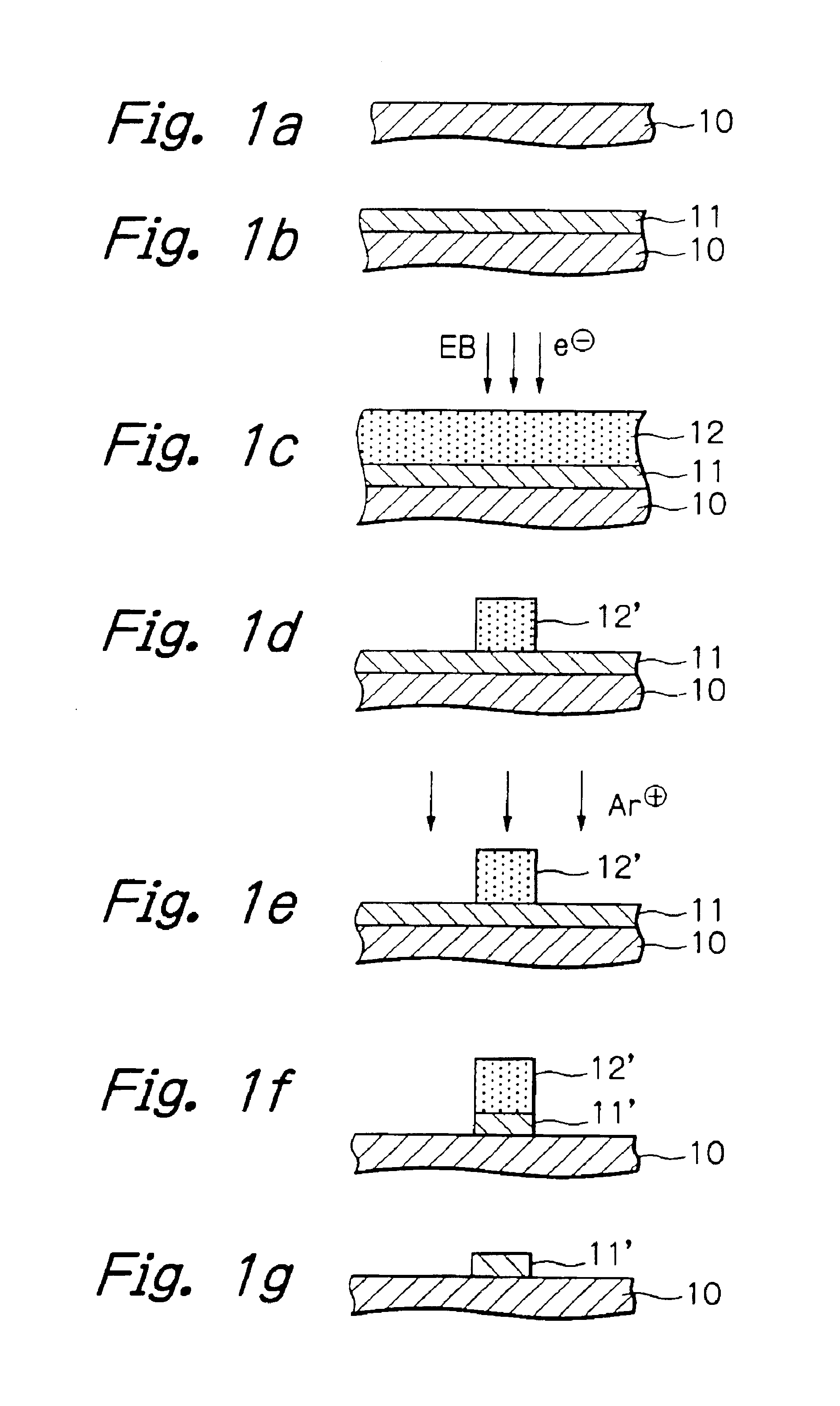
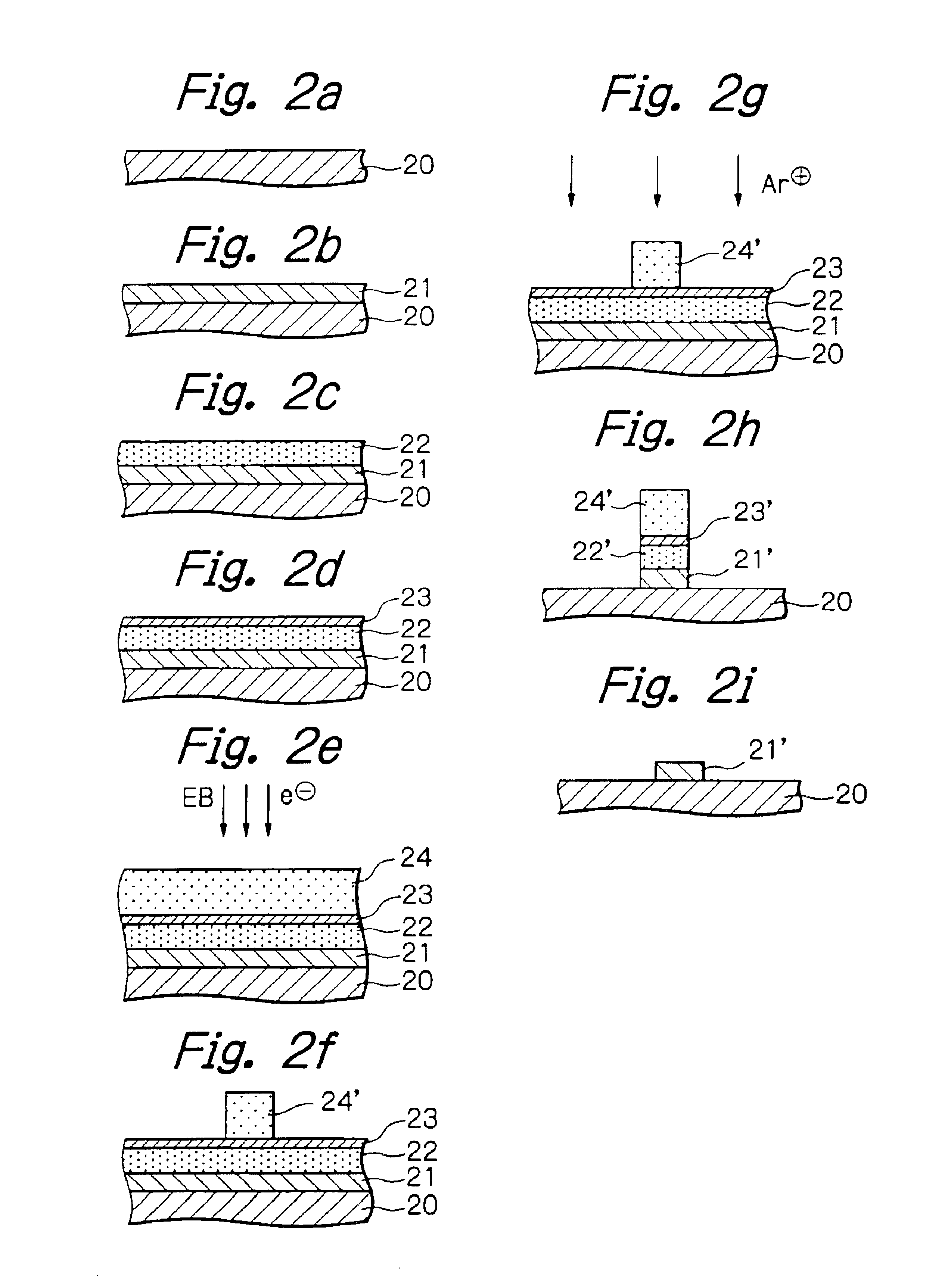
FIGS. 2a to 2i illustrate processes of a thin-film patterning in a preferred embodiment according to the present invention. In this embodiment, a resist film is cured by EB to form a resist pattern and then a thin film to be patterned is patterned by using the formed resist pattern. The thin film to be patterned may be any film applicable in a thin-film device. In a thin-film magnetic head, the thin film to be patterned may be a thin film of a magnetic pole, or a thin film or a multi-layered film of a magnetoresistive effect (MR) element for example.

As shown in FIG. 2a, first, a substrate or an under layer 20 on which a thin film to be patterned will be formed is prepared. On this substrate or under layer 20, a thin film to be patterned 21 is deposited by sputtering for example as shown in FIG. 2b.

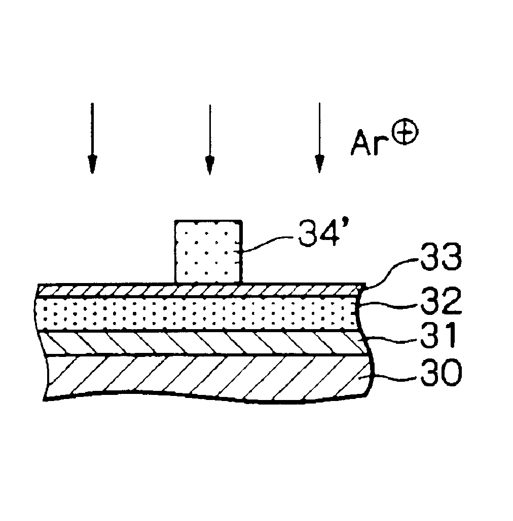
Then, as shown in FIG. 2c, an insulating organic film 22 as a strippable film is coated on the thin film 21, and, as shown in FIG. 2d, a conductive film 23 is formed on the film 22 by spu...


PUM

PropertyMeasurementUnit
insulatingaaaaaaaaaa
conductiveaaaaaaaaaa
acceleration voltageaaaaaaaaaa

Abstract

A method of patterning a thin film includes a step of forming at least one strippable conductive film on a surface of a thin film to be patterned, a step of forming a mask on the at least one strippable conductive film, a step of patterning the thin film to be patterned by dry etching using the mask, and a step of removing the at least one strippable conductive film.

Description

FIELD OF THE INVENTIONThe present invention relates to a method of patterning a thin film by using a dry etching technique or patterning a resist film by using an electron beam (EB) writing or pattern generation technique, to a method of manufacturing a thin-film device using this patterning method, and to a method of manufacturing a thin-film magnetic head using this patterning method.DESCRIPTION OF THE RELATED ARTFIGS. 1a to 1g illustrate processes, in a conventional thin-film patterning method, of forming a resist pattern on a thin-film to be patterned by using an EB writing device and of dry etching the thin-film using the resist pattern as a mask.First, on a substrate 10 shown in FIG. 1a, a thin film to be patterned 11 is deposited by for example sputtering as shown in FIG. 1b. Then, as shown in FIG. 1c, after a resist film 12 for EB writing is coated on the thin film to be patterned 11, desired regions to be remained of the resist film 12 are radiated with EB from the EB writi...

Claims


Application Information

Patent Timeline
Patent Type & Authority Patents(United States)
IPC IPC(8): C23F4/00G03F7/09G11B5/39G11B5/31H01L21/027H01L21/302H01L21/3065
CPCB82Y10/00B82Y25/00C23F4/00G03F7/091G11B5/3116G11B5/3163G11B5/3903G03F7/093G11B2005/3996
Inventor KAMIJIMA, AKIFUMI
Owner TDK CORPARATION
Why Eureka
Try Eureka