Method and apparatus for plasma etching a wafer

a technology of plasma etching and etching equipment, which is applied in the direction of pipe joints, sleeve/socket joints, electric discharge tubes, etc., can solve the problems of non-uniform etching, damage to the wafer, and increase the temperature of the wafer to an undesirable level, so as to minimize the inherent lack or excess of ions due to chamber design or process parameters, the effect of improving the uniformity of the film

Inactive Publication Date: 2005-01-04
MICRON TECH INC
View PDF22 Cites 32 Cited by
  • Summary
  • Abstract
  • Description
  • Claims
  • Application Information

AI Technical Summary

Benefits of technology

The present invention overcomes these shortcomings by providing an internally cooled rotatable chuck for use in a semiconductor wafer plasma etching apparatus. By rotating the chuck and the wafer in an etching chamber, the effect of the inherent lack or excess of ions due to chamber design or process parameters can be minimized. The lack or excess of ions creating the etch can be spread across the entire wafer surface assuring all locations see the same etch parameters. Accordingly, a more efficient process with better film uniformity will be realized.

Problems solved by technology

During plasma etching of pattern wafers, the plasma raises the temperature of the wafer to an undesirable level that could damage the wafer.
Non-uniform etching occurs, however, due to chamber design or process parameters resulting in undesirable film thickness deviations.

Method used


Image

  • Method and apparatus for plasma etching a wafer
  • Method and apparatus for plasma etching a wafer
  • Method and apparatus for plasma etching a wafer

Examples


Embodiment Construction

Further according to the invention, a method for plasma etching a wafer comprises the steps of coupling a chuck to a pedestal, coupling the wafer to the chuck, rotating the pedestal, and etching the wafer.

The present invention provides a rotatable chuck for use with apparatus for plasma etching a wafer. The invention also provides a rotatable electrostatic chuck for use with apparatus for plasma etching a patterned wafer. The invention further provides a rotatable chuck having coolant passages for conveying coolant to the chuck.

These and other features and advantages of the invention will become apparent from the following detailed description of preferred embodiments.

BRIEF DESCRIPTION OF THE DRAWINGS

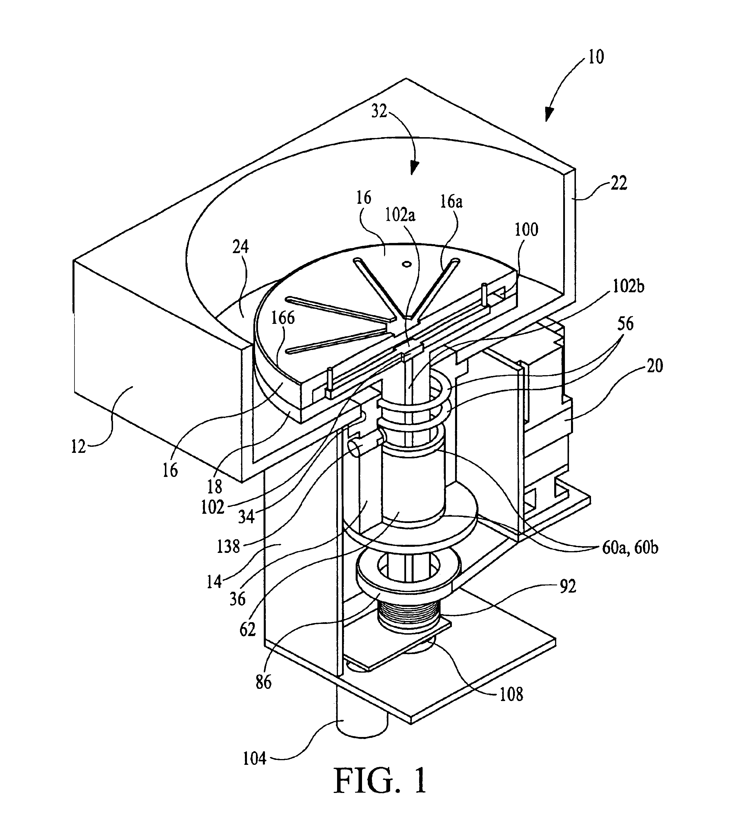
FIG. 1 is a perspective view of a plasma etching apparatus according to the present invention;

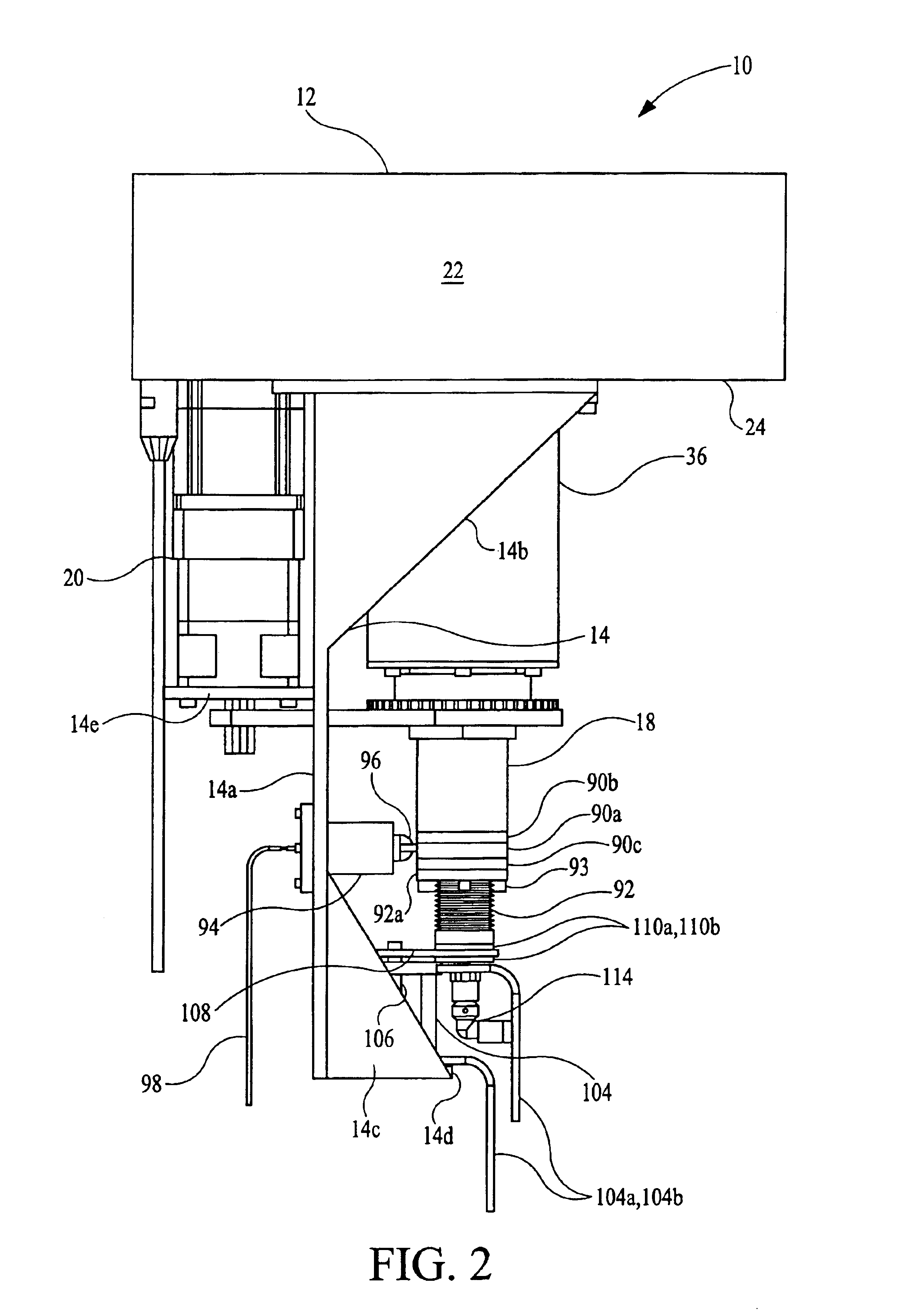
FIG. 2 is a side view of a plasma etching apparatus;

FIG. 3 is a front view of the apparatus of FIG. 2; and

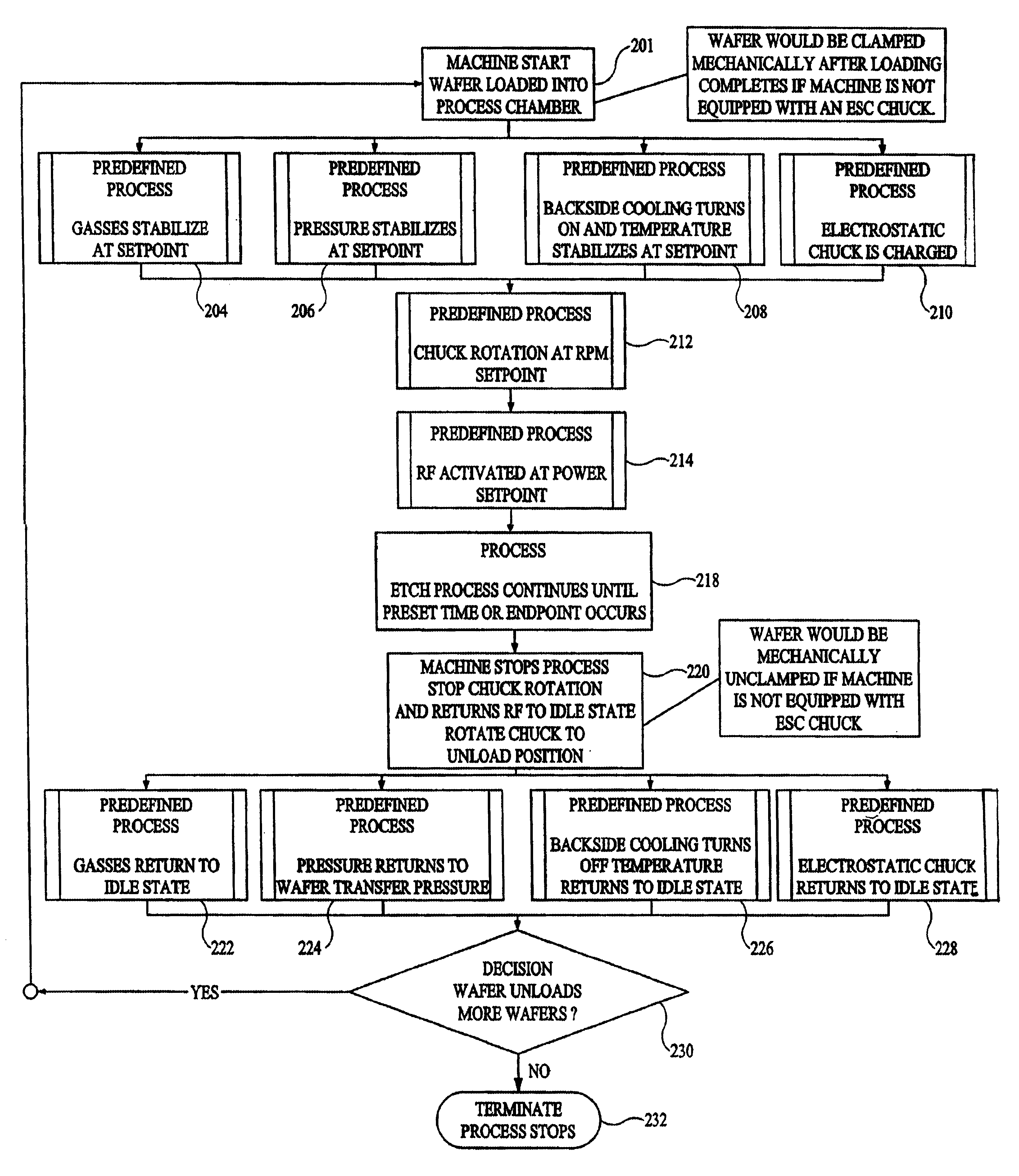
FIGS. 4, 4A and 4B are flow charts of a control process for controlling the apparatus o...


PUM


Abstract

A method utilizing a plasma etching machine which comprises a process chamber defining an interior region and including a bottom wall having an aperture and a block disposed in the aperture and including a longitudinally extending bore. A shaft extends through the bore and includes a spider push rod extending longitudinally therethrough. An internally cooled chuck is coupled to the shaft and disposed in the interior region and cooperates with the shaft to define a chamber. A spider is disposed in the chamber and is coupled to the push rod. A lift mechanism is coupled to the shaft and the push rod so that the spider pushes up on a wafer in response to actuation of the lift mechanism. A wafer clamping mechanism is coupled to the push rod if a mechanical clamp is used. In the case of electrostatic clamp the bias applied to the chuck is coupled with the use of a rotational roller to allow the bias to be applied to the chuck for the duration of the etch process. A RF source is needed for ionization of the gas. If the plasma etching machine has RF power applied through the bottom, then a rotational roller is used for this as well and must be isolated from the electrostatic voltage used to clamp the wafer.

Description

The present invention relates to a method and apparatus for plasma etching a wafer and particularly to plasma etching a wafer using a rotatable chuck. More particularly, the invention relates to an internally cooled rotatable chuck for use in a plasma etching process.BACKGROUND OF THE INVENTIONPlasma etching apparatus for processing wafers is known. Typically, a chuck serves as a lower electrode in a process chamber which can be set in a vacuum state. A wafer is placed on and fixed to the chuck, and then subjected to the plasma etching process. There are two commonly used ways of fixing a wafer to a chuck, mechanical supporting means such as a clamp, and an electrostatic chuck for attaching a wafer by means of an electrostatic attractive force. A typical electrostatic chuck includes a metallic base plate that is coated with a thick layer of slightly conductive dielectric material. A silicon wafer of approximately the same size as the chuck is placed on top of the chuck and a potenti...

Claims


Application Information

Patent Timeline
Patent Type & Authority Patents(United States)
IPC IPC(8): H01L21/00
CPCH01J37/32082H01L21/67069Y10T279/23H01J2237/2001
Inventor LANGLEY, RODNEY C.JOHNSON, DAVID R.HOFER, WILLARD L.
Owner MICRON TECH INC
Why Eureka
Try Eureka