Step-shaped floating poly-si gate to improve a gate coupling ratio for flash memory application

a floating poly-si gate and gate coupling technology, applied in the field of stacking gate flash memory, can solve the problems of increasing alone and difficulty in maintaining the same coupling level, and achieve the effects of increasing overlap area, increasing gate coupling ratio, and improving cell programming

Inactive Publication Date: 2005-01-04
TAIWAN SEMICON MFG CO LTD
View PDF13 Cites 12 Cited by
  • Summary
  • Abstract
  • Description
  • Claims
  • Application Information

AI Technical Summary

Benefits of technology

It is therefore, an object of this invention to provide a stacked-gate flash memory cell having an increased overlap area between the floating gate and the control gate with the associated increase in the gate coupling ratio for improved programming of the cell.

Problems solved by technology

As a result, it has been difficult to maintain the same coupling levels, let alone increasing them.
Although higher coupling ratios between the control gate and the floating gate can be supported by thinner inter-gate dielectric layers, or, inter-polygate oxides, data retention can cause concern due to leakages from thin layers.

Method used


Image

  • Step-shaped floating poly-si gate to improve a gate coupling ratio for flash memory application
  • Step-shaped floating poly-si gate to improve a gate coupling ratio for flash memory application
  • Step-shaped floating poly-si gate to improve a gate coupling ratio for flash memory application

Examples


Embodiment Construction

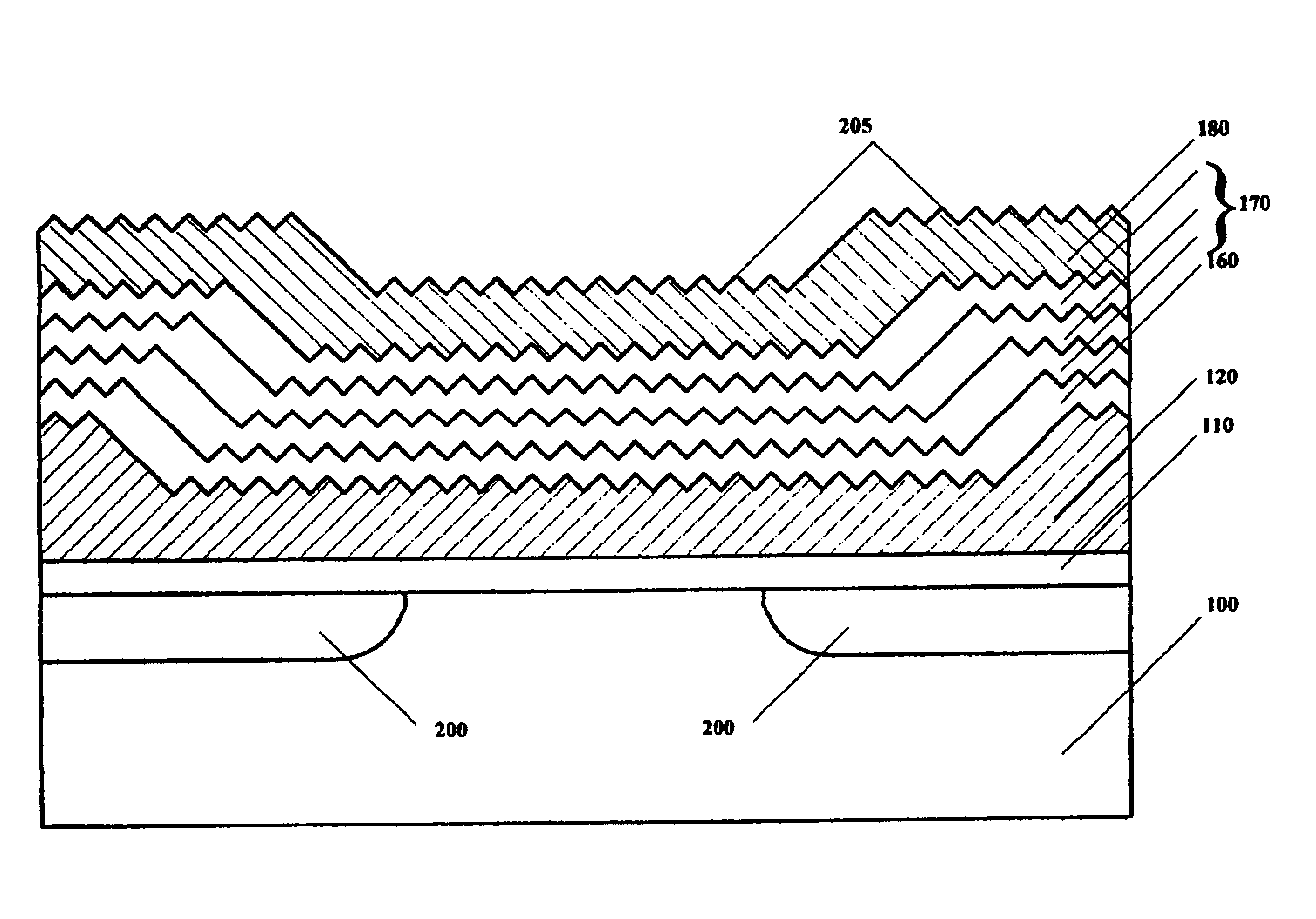
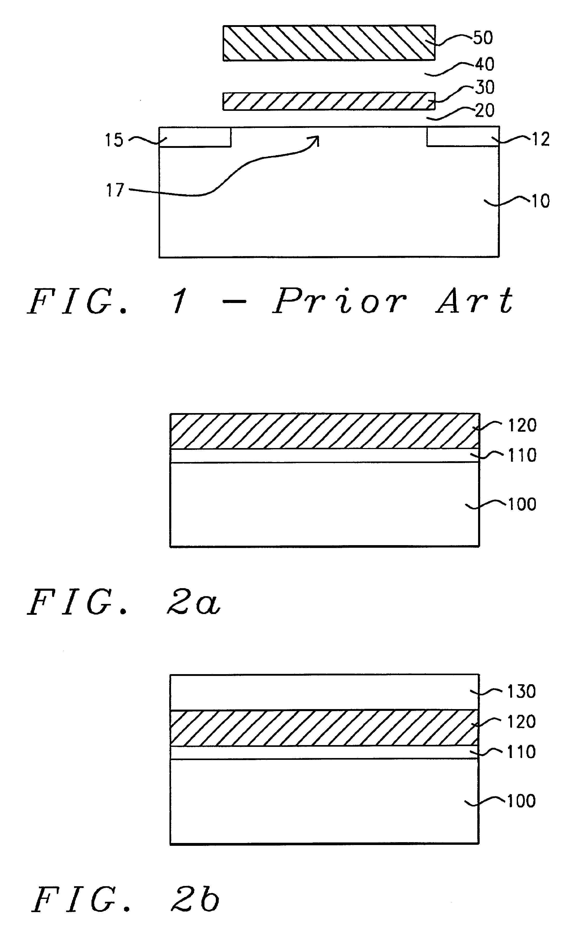
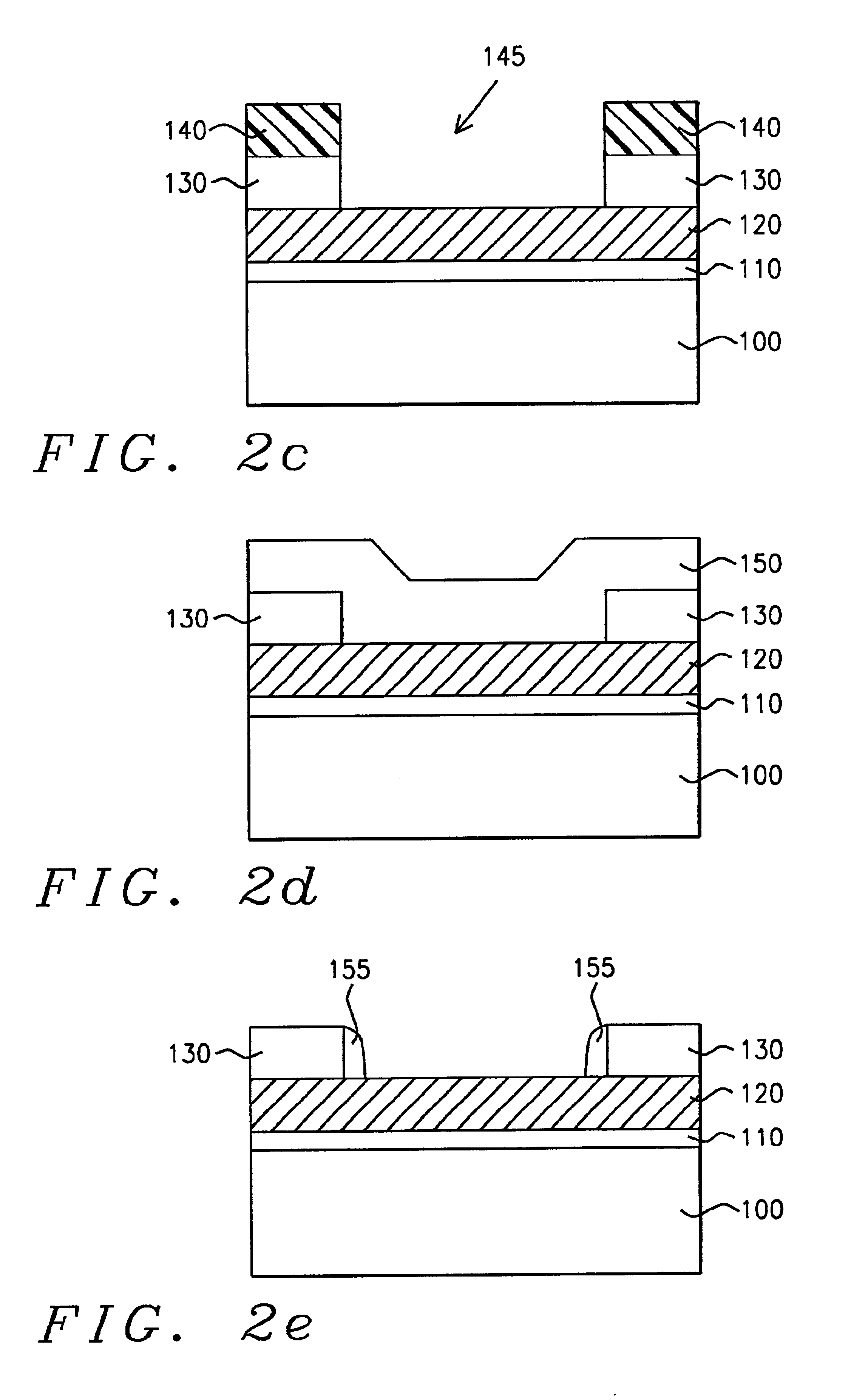
Referring now to the drawings, specifically to FIGS. 2a-2l, there is shown a preferred method of forming a stacked-gate flash memory cell having a step-shaped floating polysilicon, or, Poly-Si, gate in order to increase the coupling ratio between the floating gate and the control gate of the memory cell. It will become apparent to those skilled in the art that with the disclosure of the one continues rectangular step, other multiply connected surfaces of different shapes can also be formed on the floating gate in order to increase the coupling ratio even more. Such shapes can include triangular, or other nonuniform shapes. It will be evident that the same method disclosed here may be employed in other similar process steps of forming other shapes that are too many to cite here.

In FIG. 2a, a substrate (100), preferably silicon, is shown where a layer of gate oxide (110) is formed thereon. The preferred method of forming the gate oxide is by thermal oxidation in dry oxygen carried out...


PUM


Abstract

A stacked-gate flash memory cell is provided having step-shaped poly-gates with increased overlap area between them in order to increase the coupling ratio and hence the program speed of the cell. The floating gate is first formed with a step and the intergate dielectric is conformally shaped thereon followed by the forming of the control gate thereon. The increase in the-overlap area can be achieved by forming gates with multiply connected surfaces of different shapes.

Description

BACKGROUND OF THE INVENTION(1) Field of the InventionThe present invention relates to the manufacturing of semiconductor memories, and in particular, is directed to a stacked-gate flash memory having a step-shaped floating polysilicon gate to improve its program speed, and also to a method of forming the same.(2) Description of the Related ArtThe higher the capacitive coupling between the floating gate and the control gate of a conventional stacked-gate memory cell, the higher is the program speed of the cell, as is well-known in the art. Capacitive coupling can be increased by increasing the capacitance, through an increase in the areas of the floating and control gate electrodes on the contrary, however, because of the continued downscaling in the ultra large scale integration of semiconductor devices in general, the cell area, and hence the areas of the gate electrodes are necessarily being reduced. As a result, it has been difficult to maintain the same coupling levels, let alon...

Claims


Application Information

Patent Timeline
Patent Type & Authority Patents(United States)
IPC IPC(8): H01L29/423H01L29/40
CPCH01L29/42324
Inventor LIN, CHRONG-JUNGCHEN, SHUI-HUNG
Owner TAIWAN SEMICON MFG CO LTD
Why Eureka
Try Eureka