Plasma display panel and manufacturing method thereof

a technology of plasma display panel and manufacturing method, which is applied in the manufacture of electrode systems, electrode discharge tubes/lamps, and electrodes, etc., can solve the problems of increased production costs, long manufacturing process, and silver affecting the contrast so as to improve the brightness of plasma display panels, reduce production costs, and simplify manufacturing processes

Inactive Publication Date: 2005-01-04
LG ELECTRONICS INC
View PDF5 Cites 35 Cited by
  • Summary
  • Abstract
  • Description
  • Claims
  • Application Information

AI Technical Summary

Benefits of technology

Accordingly, it is an object of the present invention to provide a plasma display panel and a method thereof to simplify the manufacturing process by concurrently forming the black layer and the black matrix.
It is another object of the present invention to provide a plasma display panel and a method thereof to improve the brightness of the plasma...

Problems solved by technology

Such silver makes the plasma display worse in its contrast.
To this end, the manufacturing process is too long and production costs are increased.
However, as the manufacturing method of FIG. 3, the bus electrode is formed only on the transparent electrode in the discharge cell, so that it is limited to enlarge the interval between the bus electrodes in the convention plasma display panel.
If the bus electrode is formed on the non-discharge area, the silver (Ag) particle of the bus electrode migrates and bonds with the l...

Method used


Image

  • Plasma display panel and manufacturing method thereof
  • Plasma display panel and manufacturing method thereof
  • Plasma display panel and manufacturing method thereof

Examples


third embodiment

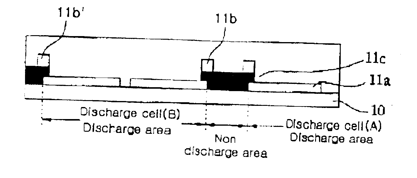
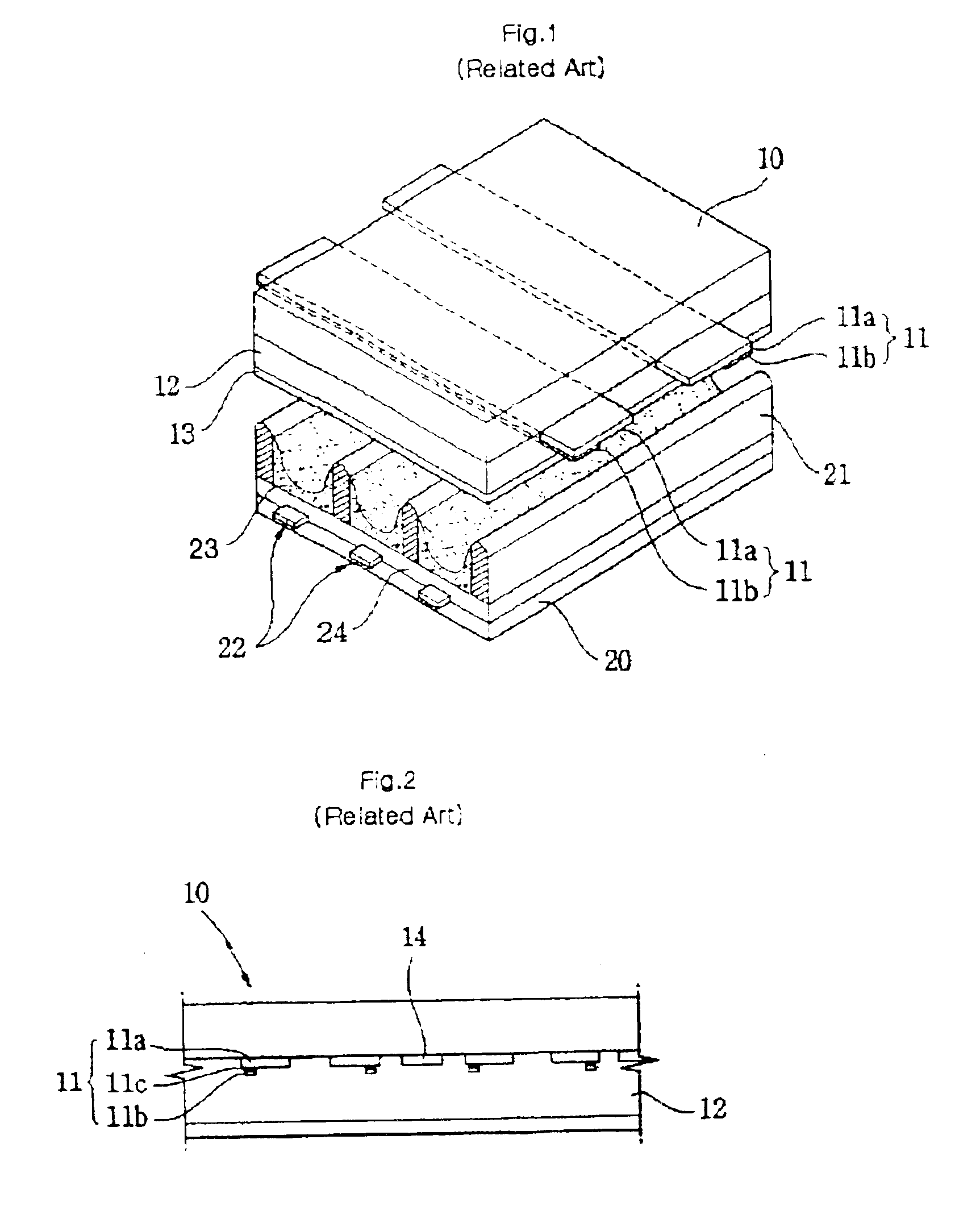
FIG. 9 shows the structure of the front substrate of the plasma display panel of the present invention. In general, the front substrate of the plasma display panel includes the discharge area where discharges occur and the non-discharge area where discharges do not occur. The non-discharge area is the area formed between the discharge cell and its adjacent discharge cell where a pair of transparent electrodes 11a are formed.

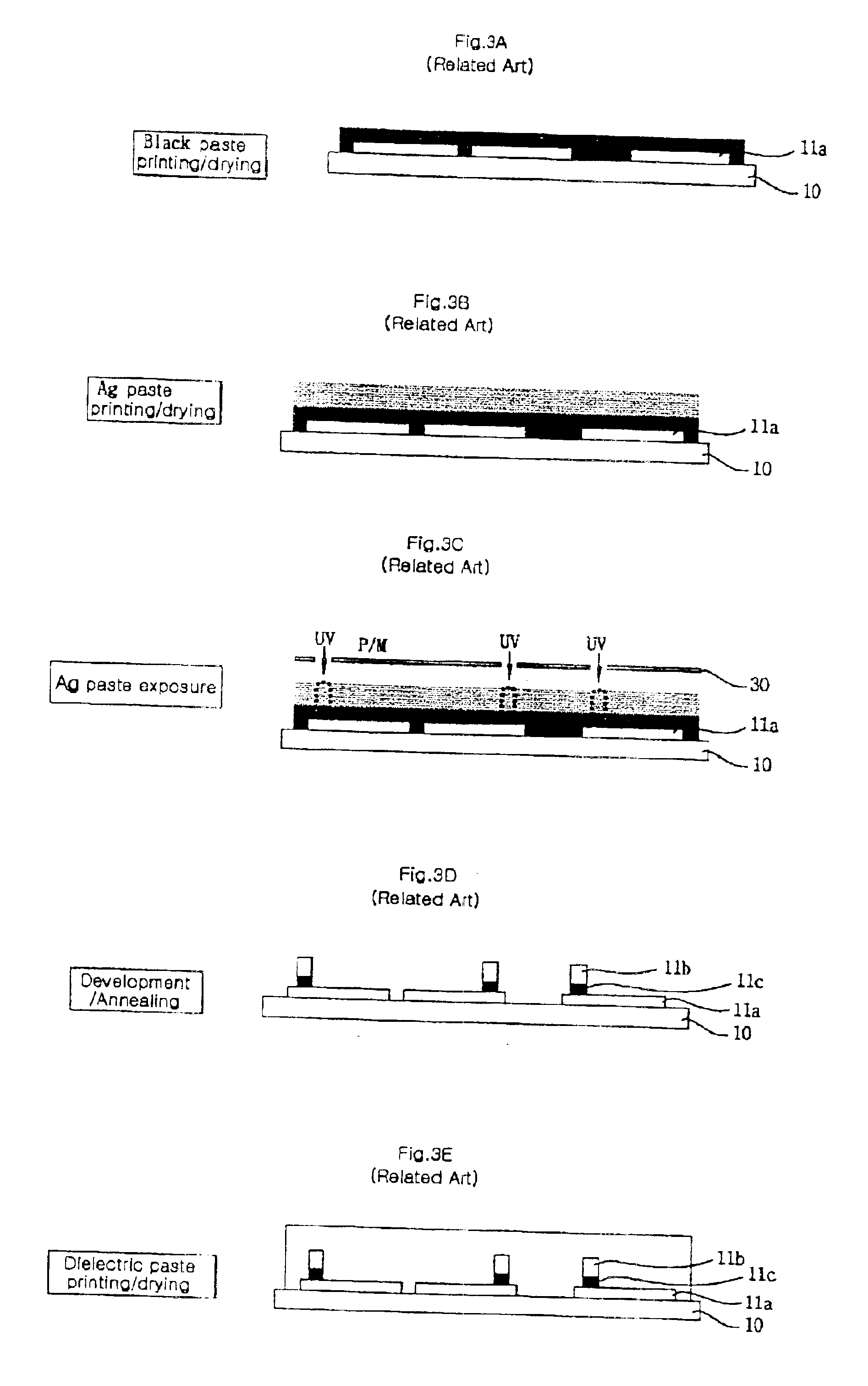
On the front substrate 10 of the plasma display panel according to third embodiment of the present invention, the black layer 11c is formed between transparent electrodes 11a and 11b and coated on the non-discharge area between the discharge cells A and B. In this case, it is desirable that the black layer formed between the non-discharge areas is a black matrix. The previous embodiment of the present invention provides that the black layer is not spaced by a constant distance from a black matrix. However, in the third embodiment of the present invention, the bl...

fourth embodiment

On the other hand, as shown in FIGS. 9 and 10A through 10F, the black layer is formed with the black matrix in one and the bus electrode 11b formed on the black layer is shifted to be formed on the non-discharge area so that the brightness can be improved. In other words, as described above, the interval between two bus electrodes 11b and 11b′ in a discharge cell is so long using a non-discharge area as a boundary as to contribute to improvement of brightness. Accordingly, two bus electrodes 11b and 11b′ in a discharge cell are formed on a portion of the adjacent non-discharge cell so that the interval between the bus electrodes 11b and 11b′ become longer to improve the brightness. This will be described referring to FIG. 11. FIG. 11 shows the structure of the front substrate of the plasma display panel according to the present invention.

Referring to FIG. 11, the black layer 11c is formed between the transparent electrode 11a and the bus electrode 11b on the front substrate 10 of th...


PUM


Abstract

The present invention relates to plasma display panel and manufacturing method thereof to simplify the manufacturing steps and reduce cost of production. In the present invention, a black layer formed between a transparent electrode and a bus electrode is formed together with a black matrix at the same time. In this case, the black layer is formed together with the black matrix in one. Cheap nonconductive oxide is used as a black powder of a black layer. Specifically, in case the black layer and the black matrix are formed in one, the bus electrode is shifted to a non-discharge area to improve the brightness of the plasma display panel.

Description

BACKGROUND OF THE INVENTION1. Field of the InventionThe present invention relates to a plasma display panel and manufacturing method thereof, and more particularly, to a front substrate of a plasma display panel capable of concurrently forming a black layer placed within a discharge and a black matrix placed between discharge cells.2. Background of the Prior ArtIn general, plasma display panel (hereafter, referred to as PDP) is a display device using the visible rays generated when vacuum ultraviolet rays generated by gas discharge excite phosphor.The PDP is thinner in thickness and lighter in weight than the cathode ray tubes (CRTs) that have been mainly employed as display devices. The PDP has an advantage in that a high definition and large-sized screen can be realized.The PDP having such advantages described above includes many discharge cells arranged in matrix fashion, and each of the discharge cells forms one pixel of a screen.FIGS. 1 and 2 show a structure of a general plasm...

Claims


Application Information

Patent Timeline
IPC IPC(8): H01J17/49H01J9/24H01J9/20H01J9/00H01J9/02H01J11/12H01J11/22H01J11/24H01J11/26H01J11/34H01J11/36H01J11/38H01J11/40H01J11/42H01J11/44
CPCH01J9/02H01J9/20H01J9/241H01J9/242H01J11/24H01J11/44H01J11/12H01J2211/444H01J2211/245
Inventor JOO, YOUNG DAECHOI, TAE WANPARK, SEUNG TEAKIM, SOON HAKKANG, SEOK DONGKIM, SANG TAEBAE, HYOUNG KYUN
Owner LG ELECTRONICS INC
Why Eureka
Try Eureka