Method of programming and erasing a non-volatile semiconductor memory

Inactive Publication Date: 2005-01-04
POWERCHIP SEMICON CORP
View PDF6 Cites 6 Cited by
  • Summary
  • Abstract
  • Description
  • Claims
  • Application Information

AI Technical Summary

Benefits of technology

The main object of the present invention is to provide a method of operating a flash mem

Problems solved by technology

It is known that a continuous ascending threshold voltage (Vth) will adv

Method used


Image

  • Method of programming and erasing a non-volatile semiconductor memory
  • Method of programming and erasing a non-volatile semiconductor memory
  • Method of programming and erasing a non-volatile semiconductor memory

Examples


Embodiment Construction

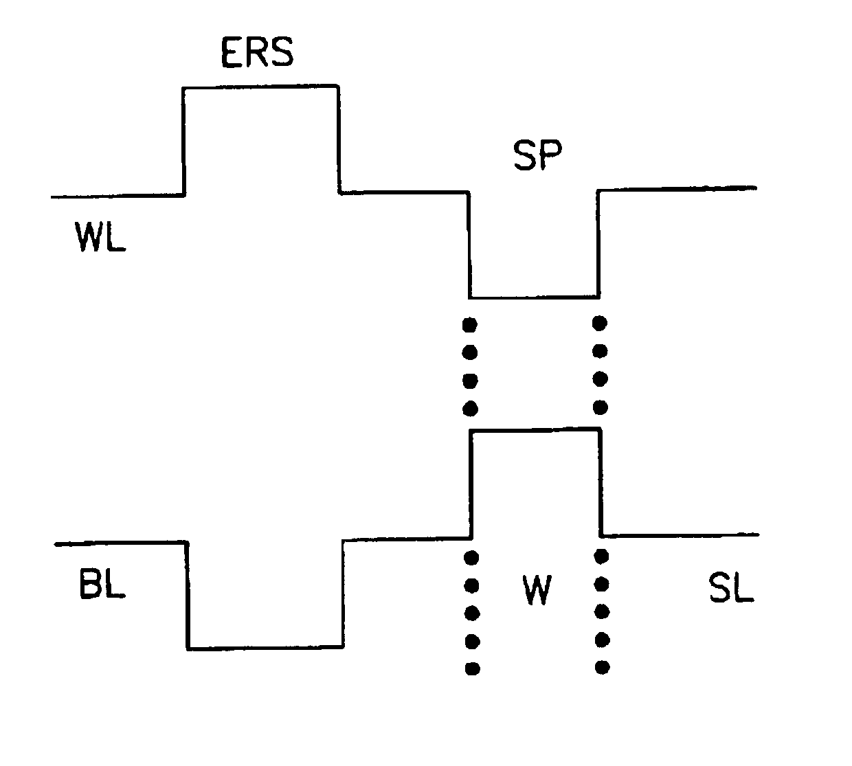
The present invention provides a method of programming flash memory with multi-level storage in the negative voltage range and erasing flash memory in the positive voltage range, as shown in FIG. 8, with enhanced conductivity and without noise disturbance.

In addition, a self-limiting means is performed along with the erasing operation (ERS) to prevent the continuous ascending of threshold voltage (Vth) as the erasing is in progress.

To this end, the memory cell structure in accordance with the present invention as shown in FIG. 9 comprises:a first conductivity substrate (10);a plurality of a second conductivity deep ion wells (12), being disposed on top of the first conductivity substrate (10);a plurality of a first conductivity shallow ion wells (14) being disposed in the second conductivity deep ion wells (12);a plurality of memory cell arrays (M) being formed over the first conductivity shallow ion wells (14);a plurality of shallow trench insulation (STI) layers (16) being dispose...


PUM


Abstract

A method of programming and erasing a non-volatile semiconductor memory is provided. The memory device for such operation has one first conductivity substrate (10), a plurality of second conductivity deep ion wells (12), a plurality of shallow ion wells (14), a plurality of memory cell arrays disposed above the shallow ion wells (14), a plurality of bit lines (BL) connected to the shallow ion wells (14) through respective conductive plugs (18), and a plurality of shallow trench insulation (STI) layers (16) above the substrate (10). The programming of memory cells with multi-level data storage takes a threshold voltage (Vth) in the negative voltage range, whilst the erasing of memory cells takes a threshold voltage (Vth) in the positive voltage range. The erasing operation is performed in conjunction with a self-limiting means to prevent continuous ascending of the threshold voltage (Vth) as the erasing operation is in progress.

Description

BACKGROUND OF THE INVENTION1. Field of the InventionThe present invention relates to a method of programming and erasing a non-volatile semiconductor memory, in particular to a method of operating the flash memory that is capable of supporting multi-level data storage with enhanced conductivity and without noise disturbance.2. Description of Related ArtsProgramming and erasing of a flash memory is usually performed by channel hot electron (CHE) or Fowler-Nordheim tunneling (FN tunneling). However, using CHE to write into memory cells usually requires excessively high power consumption. The industry has therefore developed a NAND flash memory that is operated with low power.The structure of a memory cell (70) in a conventional NAND flash memory, as shown in FIG. 1, comprises:a p-well (72);an n-source (74) formed on top of the p-well (72);an n-drain (76) formed on top of the p-well (72) corresponding to the position of the n-source (74);a stacked gate (80), formed on the surface of th...

Claims


Application Information

Patent Timeline
IPC IPC(8): G11C11/56G11C16/12G11C16/14G11C16/06
CPCG11C11/5628G11C16/14G11C16/12G11C11/5635
Inventor YANG, CHING-SUNGCHANG, HSIANG-CHUNG
Owner POWERCHIP SEMICON CORP
Why Eureka
Try Eureka