Semiconductor device and method of fabricating semiconductor device with high CMP uniformity and resistance to loss that occurs in dicing

a semiconductor device and uniformity technology, applied in the field of semiconductor devices, can solve the problems of increased loss, increased loss, and sparse arrangement of dummy patterns, and achieve the effect of superior loss resistan

Active Publication Date: 2005-01-11
RENESAS ELECTRONICS CORP
View PDF7 Cites 294 Cited by
  • Summary
  • Abstract
  • Description
  • Claims
  • Application Information

AI Technical Summary

Benefits of technology

It is an object of the present invention to provide a semiconductor device and a method of fabricating a semiconductor device in which dummy patterns are evenly formed in chip interior areas, and moreover, in which dummy patterns having superior resistance to loss when dicing are formed in scribe line areas.

Problems solved by technology

The occurrence of nonuniformity in the pattern that is formed on the cutting space of this cutter causes variation in the hardness of the wafer encountered by the cutter, and this variation tends to cause loss during cutting.
In particular, when the pattern is scattered, the hardness is uniform in that portion, and loss that has once occurred tends to spread over a large area, resulting in an expanded area of loss.
A construction having the “diagonally forward skipped arrangement” described hereinabove entails an increased probability that the arrangement of the dummy pattern will become sparse with respect to the direction of advance of the cutter and that a greater loss will thus occur.
Typically, a film having a low dielectric constant itself has a low level of hardness, and further, has a low level of adhesion to the silicon oxide films or silicon nitride films that have been used conventionally as interlayer insulating films, and the use of a film having a low dielectric constant as the insulating film between wiring layers will therefore result in more extreme loss during dicing.
Nevertheless, the arrangement of dummy patterns in grid form over the entire surface of a wafer causes unevenness in the arrangement of the dummy patterns within the chip areas.

Method used


Image

  • Semiconductor device and method of fabricating semiconductor device with high CMP uniformity and resistance to loss that occurs in dicing
  • Semiconductor device and method of fabricating semiconductor device with high CMP uniformity and resistance to loss that occurs in dicing
  • Semiconductor device and method of fabricating semiconductor device with high CMP uniformity and resistance to loss that occurs in dicing

Examples


Embodiment Construction

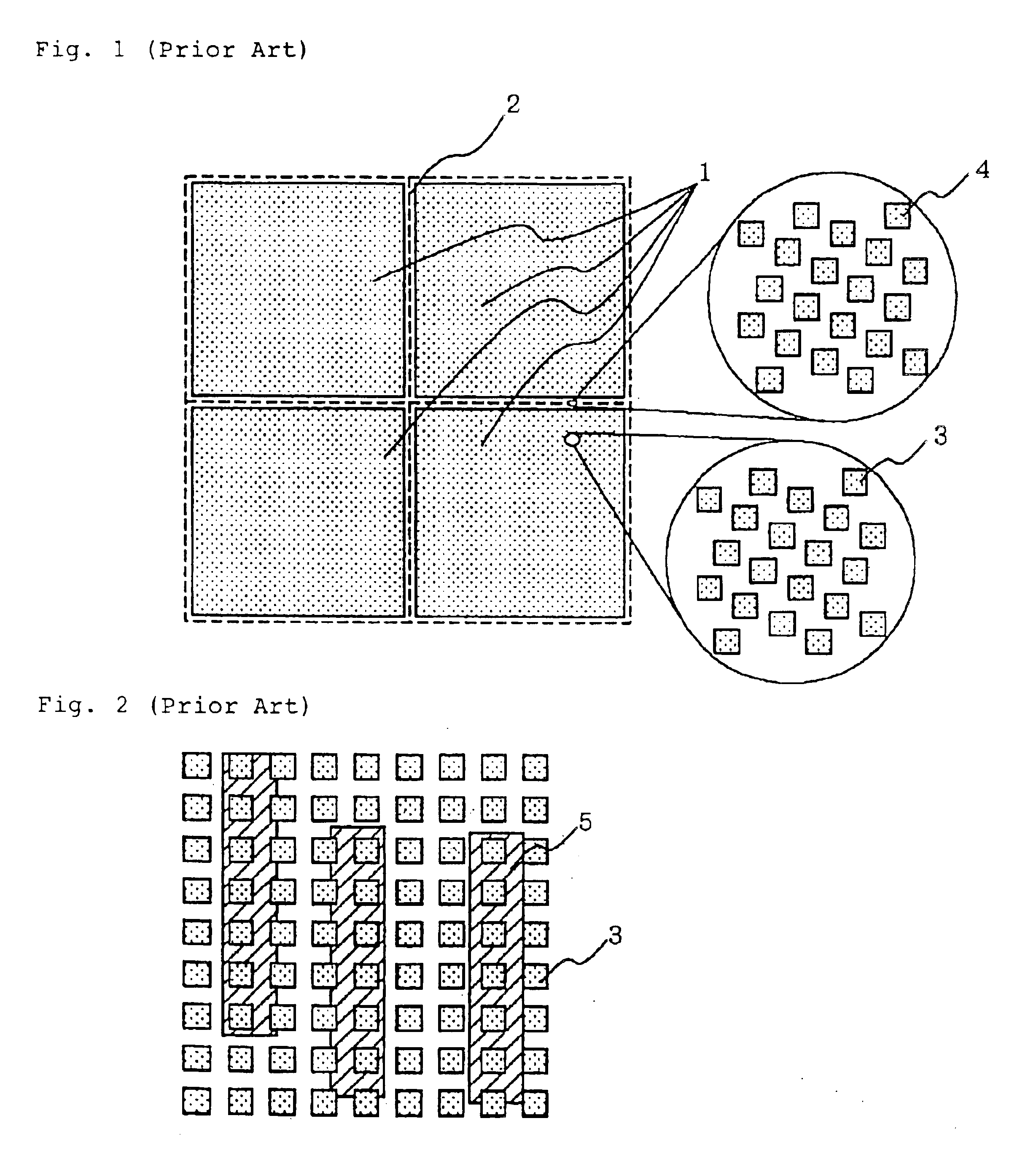
FIG. 5 is a plan view showing the arrangement of dummy pattern wiring in a semiconductor device according to the first embodiment of the present invention, and in particular, in a semiconductor device that uses a trench construction for forming wiring lines.

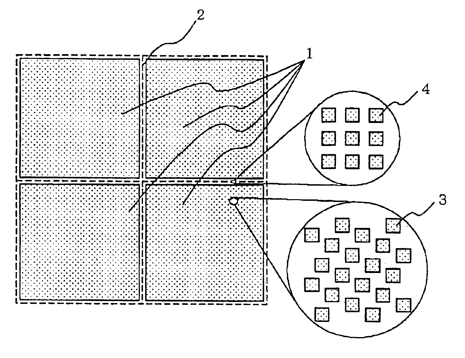
Referring to FIG. 5, scribe line areas 2 having a width of 100 μm are provided around the peripheries of chip areas 1 that have been formed on a silicon wafer. Dummy patterns 3 having a square shape measuring 2 μm on each side are arranged in the “diagonally forward skipped arrangement” in chip areas 1.

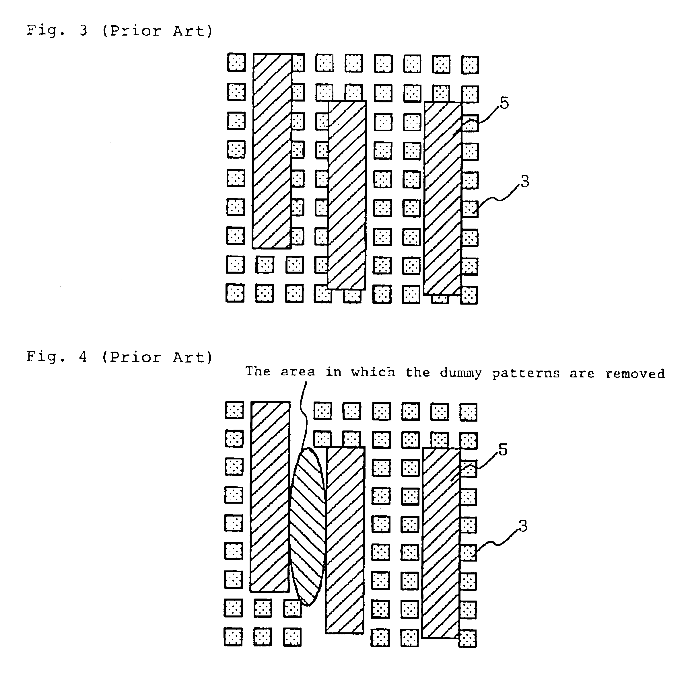
More specifically, as shown in FIG. 6, dummy patterns 3 are arranged within grids that are repeated horizontally and vertically over the entire surface of chip areas 1, one grid being made up by 5 by 5 squares (a total of 25 squares) each square measuring 1.7 μm on a side arranged horizontally and vertically. In this arrangement, dummy patterns 3 are not uniformly arranged in the vertical direction, horizontal direction, and 45 deg...


PUM


Abstract

In the semiconductor device of the present invention, a plurality of dummy patterns are formed in a grid arrangement in the scribe line areas of a wafer, and a plurality of dummy patterns are formed in a diagonally forward skipped arrangement in the chip interior areas of the wafer. Altering the arrangement of dummy patterns in the chip interior areas and scribe line areas in this way enables formation of dummy patterns with greater uniformity in the chip interior areas and enables formation of dummy patterns with greater resistance to loss that occurs when dicing in scribe line areas.

Description

BACKGROUND OF THE INVENTION1. Field of the InventionThe present invention relates to a semiconductor device and to a method of fabricating the device; and more particularly to a semiconductor device on which dummy patterns are formed on a wiring layer and to the method of fabricating the device.2. Description of the Related ArtIn a conventional method of fabricating a semiconductor device having a multiple interconnection layers, when a method is adopted in which a wiring layer is formed by filling trenches with a metal, CMP (Chemical Mechanical Polishing) is used to remove unnecessary metal except the metal that has been embedded in the trenches. In such a case, a wiring pattern that has been formed unevenly on the wafer will cause variation in the polishing speed, and a countermeasure therefore is necessary for limiting variation in the film thickness of the wiring that is finally formed. For this purpose, a method has been conventionally adopted in which dummy patterns are arrang...

Claims


Application Information

Patent Timeline
Patent Type & Authority Patents(United States)
IPC IPC(8): H01L21/02H01L21/301H01L23/544H01L21/44H01L21/70H01L23/48H01L21/822H01L21/3205H01L21/321H01L21/768H01L21/82H01L21/78H01L27/04H01L23/52H01L23/58
CPCH01L21/78H01L23/585H01L21/7684H01L2924/0002H01L2924/00
Inventor MATSUMOTO, AKIRAFUKASE, TADASHIIGUCHI, MANABU
Owner RENESAS ELECTRONICS CORP
Why Eureka
Try Eureka