Elastomer interposer for grid array packages and method of manufacturing the same

a technology of elastomer interposers and grid arrays, applied in the field of elastomer interposers, can solve the problems of poor humidity resistance reliability and introduction of short circuits, and achieve the effect of enhancing package reliability and facilitating electrical connections

Inactive Publication Date: 2005-01-11
VIA TECH INC
View PDF11 Cites 20 Cited by
  • Summary
  • Abstract
  • Description
  • Claims
  • Application Information

AI Technical Summary

Benefits of technology

It is therefore an objective of this invention to provide an elastomer interposer employed between a package and a printed circuit board, and the method of manufacturing the same. The elastomer interposer design of the present invention not only facilitates the electrical connection between the package and the PCB, but also protects the components in the package from destruction by the external force. Additionally, the elastomer interposer functions as a strain reliever for the solder balls between the package and the PCB, thus greatly enhance the reliability of the package against thermal cycle failure. Besides, the elastomer interposer could be electrically connected to the package and the PCB by the solder balls or the conductive bumps, depending on the applied package and PCB styles.

Problems solved by technology

Also, no surface insulating layer is adopted in the elastomeric connector 402 to isolate adjacent surface conductor tabs 410, and this may easily introduce short circuit and poor humidity resistance reliability.

Method used


Image

  • Elastomer interposer for grid array packages and method of manufacturing the same
  • Elastomer interposer for grid array packages and method of manufacturing the same
  • Elastomer interposer for grid array packages and method of manufacturing the same

Examples


first embodiment

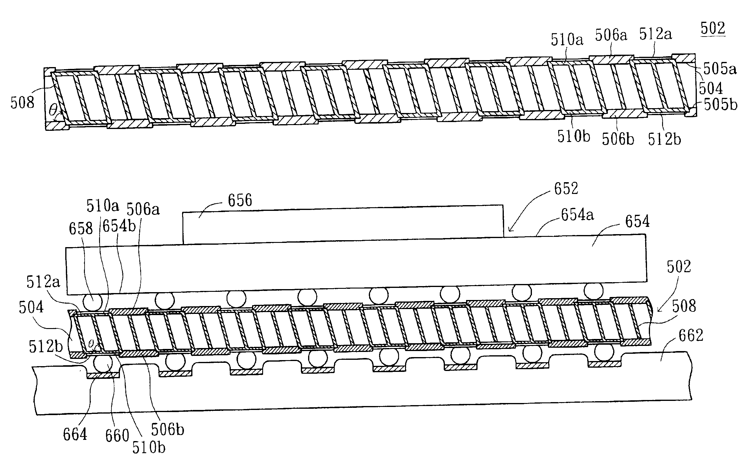
FIG. 5A is a cross-sectional drawing of an elastomer interposer according to the first embodiment of the invention. The elastomer interposer 502 includes an elastomer 504, the solder resistant layers (insulating layers) 506a and 506b, numerous parallel, conductive wires 508, the conductive pads and solder ball pads, wherein the conductive pads could be the Cu pads 510a and 510b, the solder ball pads could be the Ni / Au plated pads 512a and 512b for the improvement of electrical connection and solder joint reliability. The elastomer 504 having the top surface 505a and bottom surface 505b in parallel provides the flexibility of elastomer interposer 502. The solder resistant layer 506a having openings surrounding the Ni / Au plated pads 512a are on the top surface 505a of the elastomer 504, while the solder resistant layer 506b having openings surrounding Ni / Au plated pads 512b are on the bottom surface 505b of the elastomer 504.

Also, the Cu pads 510a are plated to become the Ni / Au plated...

example 1

FIG. 7 is a cross-sectional drawing of the elastomer interposer employed between the PCB and CBGA package according to example 1 of the first embodiment of the invention. In FIG. 7, the CBGA (ceramic ball grid array) package 652 includes a CBGA substrate 654 and a ceramic lid 656. The ceramic lid 656 formed over the top surface 654a of the CBGA substrate 654 functions as a hermetic seal. The solder balls 658 attached to the bottom surface 654b of the CBGA substrate 654 are soldered to the Ni / Au plated pads 512 at high temperature, and make a electrical connection between the CBGA package 652 and the elastomer interposer 502. Also, numerous solder balls 660 are attached to the Ni / Au plated pads 512b and soldered to the solder ball pads 664 on the PCB 662, to make an electrical connection between the elastomer interposer 502 and the PCB 662.

The coefficient of thermal expansion (CTE) of the CBGA substrate 654 is approximately 8 ppm / ° C.; while the CTE of the PCB 662 is approximately 18...

example 2

FIG. 8 is a cross-sectional drawing of the elastomer interposer employed between the low-CTE PCB and PBGA package according to example 2 of the first embodiment of the invention. In FIG. 8, the PBGA (plastic ball grid array) package 702 includes a PBGA substrate 704 and a molding compound 706. The molding compound 706 is formed over the top surface 704a of the PBGA substrate 704 and maintains the electric connection between the IC and the PBGA substrate 704. The solder balls 708 attached to the bottom surface 704b of the PBGA substrate 704 are soldered to the Ni / Au plated pads 512a of the elastomer interposer 502 at high temperature, and make an electrical connection between the PBGA package 702 and the elastomer interposer 502. Also, numerous solder balls 710 attached to the Ni / Au plated pads 512b are soldered to the solder ball pads 714 on the PCB 712, to make an electrical connection between the elastomer interposer 502 and the PCB 712.

The CTE of the PBGA substrate 704 is approxi...


PUM


Abstract

An elastomer interposer employed between a package and a printed circuit board and the method of manufacturing the same are disclosed. The elastomer interposer includes an elastomer, a plurality of conductive wires, Cu pads, solder resistant blocks and Ni / Au plated pads. The elastomer has two contact surfaces. The conductive wires are arranged inside the elastomer at a certain interval and tilted toward one of the contact surfaces with an inclined angle. The Cu pads are formed on both of the surfaces at a space, and electrically connected to the corresponding conductive wires. Also, the Ni / Au plated pads are formed over the Cu pads.

Description

This application incorporates by reference of Taiwan application Serial No. 091102286, filed Feb. 7, 2002.BACKGROUND OF THE INVENTION1. Field of the InventionThe invention relates in general to an elastomer interposer employed between the package and PCB and the method of manufacturing the same, and more particularly to an elastomer interposer functioning as a strain reliever for the solder balls between the package and the PCB, thus greatly enhance the reliability of the package against the thermal cycle failure.2. Description of the Related ArtThe integrated circuit (IC) devices can be packaged by a variety of the exterior packaging materials, so that IC can be mounted on the printed circuit board (PCB) and the functions of IC and heat dissipation are also achieved. In assembling IC onto the PCB, the conventional method of pin through hole (PTH) is mostly replaced by the surface mount technology (SMT), in order to increase the assembly efficiency and density of IC package.The PTH ...

Claims


Application Information

Patent Timeline
Patent Type & Authority Patents(United States)
IPC IPC(8): H01L23/48H01L23/498H05K3/40H05K3/34
CPCH01L23/49827H05K3/4038H05K3/3436H01L2224/32225H01L2224/45144H01L24/48H05K2203/0235H05K2201/10378H05K2201/10287H05K2201/09836H05K2201/0133H01L2924/15311H01L2924/01079H01L2924/01078H01L2224/48091H01L2224/48227H01L2224/48228H01L2224/73265H01L2924/00014H01L2924/00012H01L2924/00H01L24/45H01L2924/181H01L2224/48237H01L24/73H01L2924/14H01L2924/15183Y02P70/50H01L2924/00015
Inventor CHIEN, RAY
Owner VIA TECH INC
Why Eureka
Try Eureka