Semiconductor memory device with clock generating circuit

Inactive Publication Date: 2005-01-11
RENESAS TECH CORP
View PDF2 Cites 71 Cited by
  • Summary
  • Abstract
  • Description
  • Claims
  • Application Information

AI Technical Summary

Benefits of technology

The present invention has been made to solve the problem and it is an object of the present invention to provide a semiconductor m

Problems solved by technology

This is because a delay generates in a period after an external clock is inputted to a semiconductor memory device till data is actually outputted, because of capacitance of internal circuits in the semiconductor memory device.
However, since the time in which DLL clocks are transmitted to various circuits af

Method used


Image

  • Semiconductor memory device with clock generating circuit
  • Semiconductor memory device with clock generating circuit
  • Semiconductor memory device with clock generating circuit

Examples


Example

First Embodiment

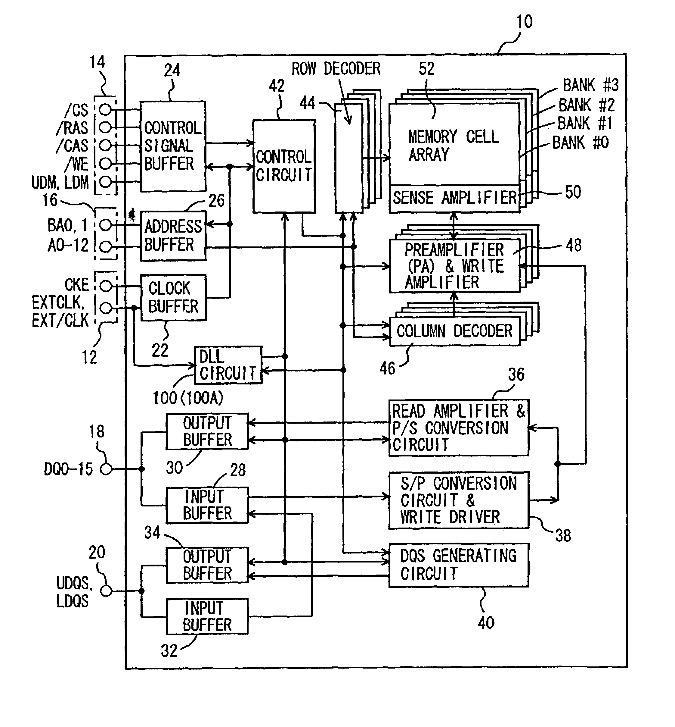
FIG. 1 is an overall block diagram schematically showing a configuration of a semiconductor memory device according to the present invention.

Referring to FIG. 1, a semiconductor memory device 10 includes: a clock terminal 12; a control signal terminal 14; an address terminal 16: a data input-output terminal 18 and a data strobe signal input-output terminal 20.

Semiconductor memory device 10 further includes: a clock buffer 22; a control signal buffer 24; an address buffer 26: an input buffer 28 and an output buffer 30 related to data DQ0 to DQ15; and an input buffer 32 and an output buffer 34 related to data strobe signals UDQS and LDQS.

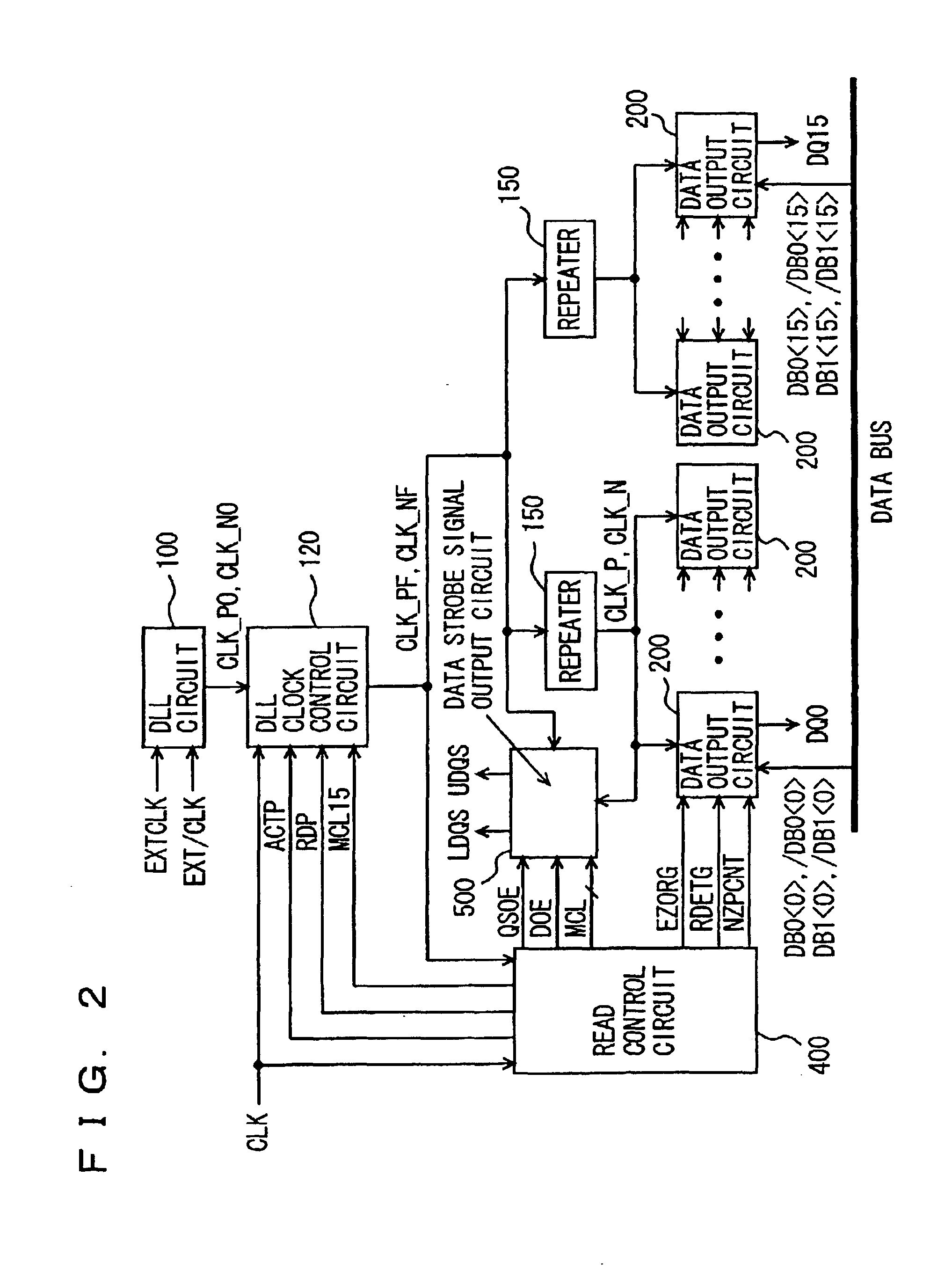
Semiconductor memory device 10 further includes: a read amplifier & P / S (parallel / serial) conversion circuit 36; an S / P (serial / parallel) conversion circuit & write driver 38; a DQS generating circuit 40; and a DLL circuit 100.

Semiconductor memory device 10 further includes: a control circuit 42; a row decoder 44; a column decoder 46; ...

Example

As described above, since semiconductor memory device 10 according to the first embodiment 10 is installed with DLL clock control circuit 120 controlling transmission of DLL clocks CLK_PE and CLK_NF based on a detected operating frequency, DLL clocks CLK_PE and CLK_NF are transmitted only in a proper period according to an operating environment; thereby achieving reduction in active standby current and stabilization of data output operation.

According to semiconductor memory device 10, in a case where an operating frequency is low, since DLL clocks CLK_PF and CLK_NF are transmitted after READ command is received, power consumption during active standby is reduced, while in a case where an operating frequency is high, since DLL clocks CLK_PF and CLK_NF are transmitted when and after ACT command is received, a data output operation is guaranteed.

Furthermore according to semiconductor memory device 10, DLL clock control circuit 120 detects an operating frequency and determines whether o...

Example

Second Embodiment

In the first embodiment, determination of a frequency is performed during a period when signal EN is at H level in frequency determining circuit 1202, and signal EN is a signal having a cycle obtained by dividing a cycle of internal clock CLK_PO into halves (a half cycle of internal clock CLK_PO) with frequency dividing circuit 1212 of frequency determining circuit 1202. The number of frequency divisions determines a sampling frequency at which a frequency determination is performed, and the reason why a signal obtained by dividing a frequency of internal clock CLK_PO in such a way is that power consumption in frequency determination circuit 1202 is reduced. In the second embodiment, the number of frequency divisions is set to larger in order to decrease power consumption in frequency determining circuit 1202.

FIGS. 29 to 32 are circuit diagrams showing configurations of frequency dividing circuits included in frequency determining circuits in a semiconductor memory ...


PUM


Abstract

A DLL clock control circuit determines whether or not an operating frequency is a low frequency satisfying a prescribed condition, based on signals received from a DLL circuit and a READ control circuit. When the DLL clock control circuit determines that the operating frequency is a low frequency, the DLL clock control circuit outputs a DLL clock received from the DLL circuit if a first signal to be activated in response to a READ command is activated, while when determining that an operating frequency is not a low frequency, outputting a DLL clock received from the DLL circuit if a second signal to be activated in response to an ACT command is activated. As a result, a semiconductor memory device can guarantees a data output operating in data reading and can reduce power consumption during active standby.

Description

BACKGROUND OF THE INVENTION1. Field of the InventionThe present invention relates to a semiconductor memory device, and more particularly to a semiconductor memory device which operates in synchronization with a rise and fall of an external clock and which includes a clock generating circuit generating an internal clock in synchronization with the external clock.2. Description of the Background ArtIn a synchronous dynamic random access memory (hereinafter, referred to as SDRAM) operating in synchronization with an external clock supplied externally, a clock generating circuit is installed inside SDRAM and an internal clock in synchronization with the external clock is generated in the clock generating circuit to perform an input-output operation of data using the internal clock. Therefore, an input-output timing of data is largely affected by a phase accuracy of the internal clock thereon.In recent years, by the demand for a higher frequency operation of a semiconductor memory devic...

Claims


Application Information

Patent Timeline
IPC IPC(8): G11C7/00G11C7/22G11C11/407G11C11/4076G11C11/409
CPCG11C7/1066G11C7/22G11C11/4076G11C7/222G11C2207/2227
Inventor KONO, TAKASHI
Owner RENESAS TECH CORP
Why Eureka
Try Eureka