Device and method for analyzing EMI noise and semiconductor device

a technology of emi noise and semiconductor devices, applied in semiconductor/solid-state device testing/measurement, instruments, analogue processes for specific applications, etc., can solve the problems of increasing the densities of integrated circuits, affecting the performance of semiconductor devices, and emi noise emission substantially problematic, so as to reduce the noise effect of emi nois

Inactive Publication Date: 2005-01-11
KK TOSHIBA
View PDF9 Cites 48 Cited by
  • Summary
  • Abstract
  • Description
  • Claims
  • Application Information

AI Technical Summary

Benefits of technology

It is an object of the present invention to provide a device and a method for analyzing EMI noise in accordance with which the reduction of EMI noise as generated from the electric power system of semiconductor device can be effectively conducted.

Problems solved by technology

Recently, emission of EMI noise becomes substantially problematic while the packing densities of integrated circuits have been increased.
However, in the case of the prior art technique, the noise level can be evaluated only by actually fabricating the integrated circuit and measuring the electric current as output from the terminals of the integrated circuit.
It is, however, difficult to analyze the current flows and the spectral components of the electric current at the respective nodes inside of the integrated circuit since the information about the current flows is not available by means of actual measurement.
However, these conventional techniques are directed to the analysis of the voltage drop and the electromigration of the power system but not provided for the analysis of the spectral components of the electric currents and the current paths of power supply systems.
Namely, it is impossible to analyze the spectral components of the electric current in the power system, since the conventional technique is not directed to the measure to reduce EMI noise.
However, it is difficult to accurately determine the capacitance and the inductance of the LC circuit in accordance with the technique as proposed.
For this reason, in order to determine the respective value of R, L and C to be inserted by the prior art technique, actual measurement nas to be repeated with a number of variations of the respective values, resulting in the problem that it takes much labor time and costs as required.
However, in this case, insertion of a large resistor possibly entails an undesirable power voltage drop.
Because of this, in order to determine the resistance value of the resistor, actual measurement has to be repeated with a number of variations of the resistance values, resulting in the problem that it takes much lator time and costs as required.

Method used


Image

  • Device and method for analyzing EMI noise and semiconductor device
  • Device and method for analyzing EMI noise and semiconductor device
  • Device and method for analyzing EMI noise and semiconductor device

Examples


embodiment 1

[EMBODIMENT 1]

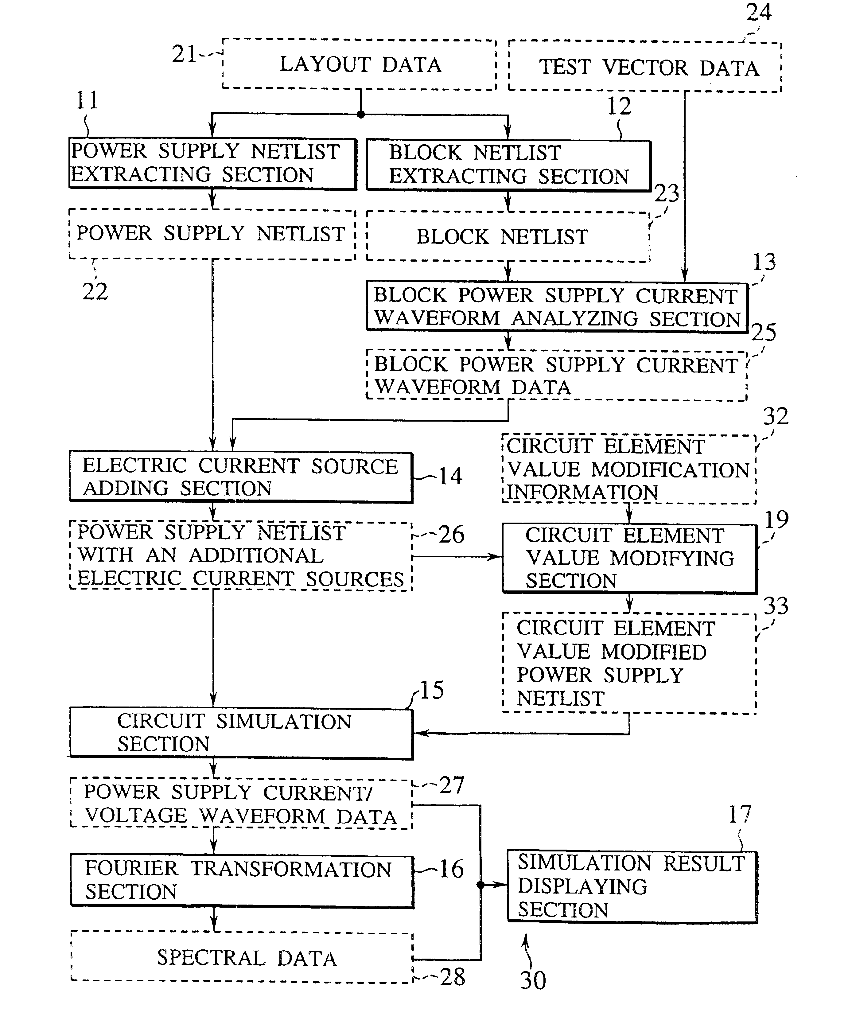
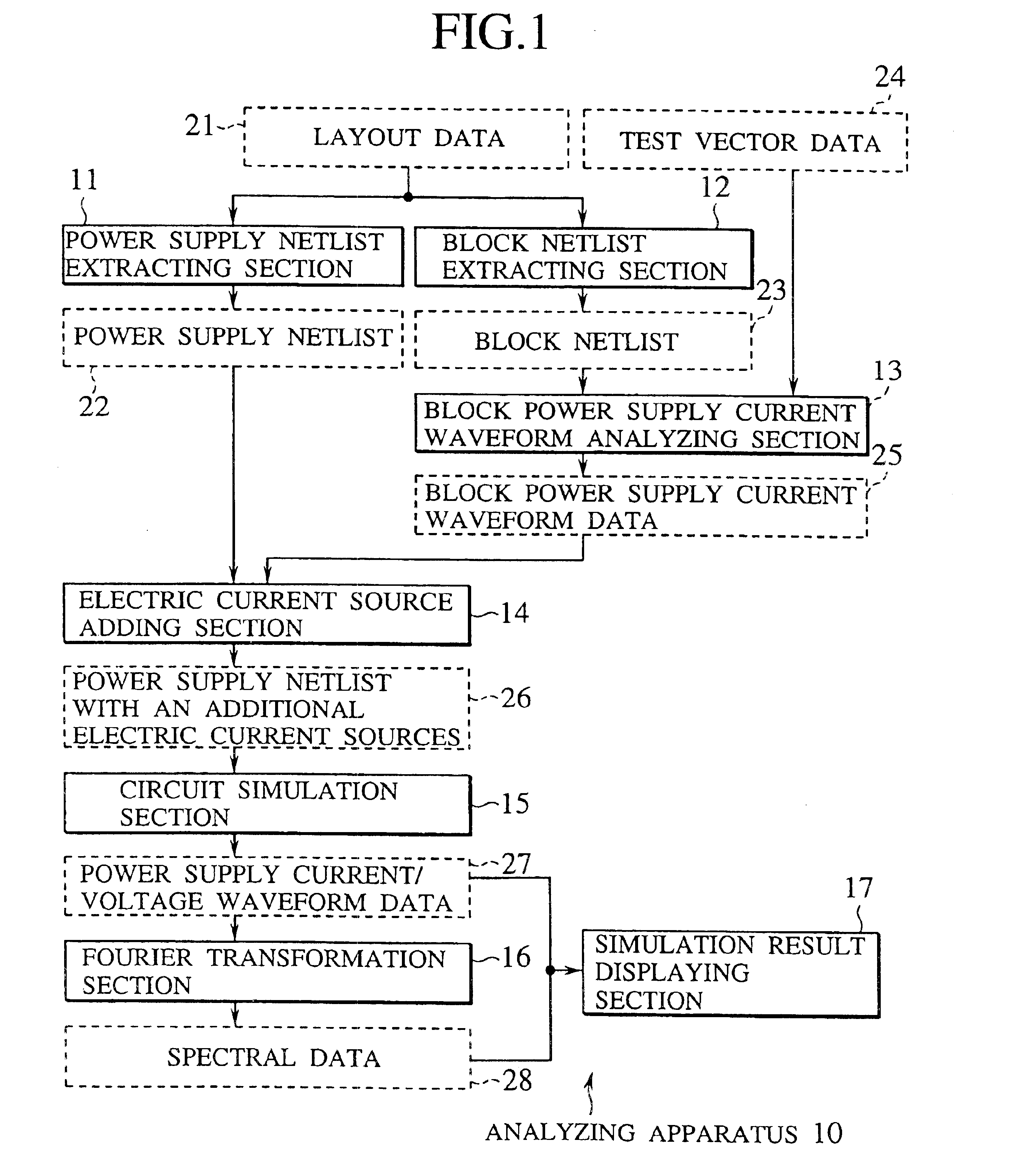
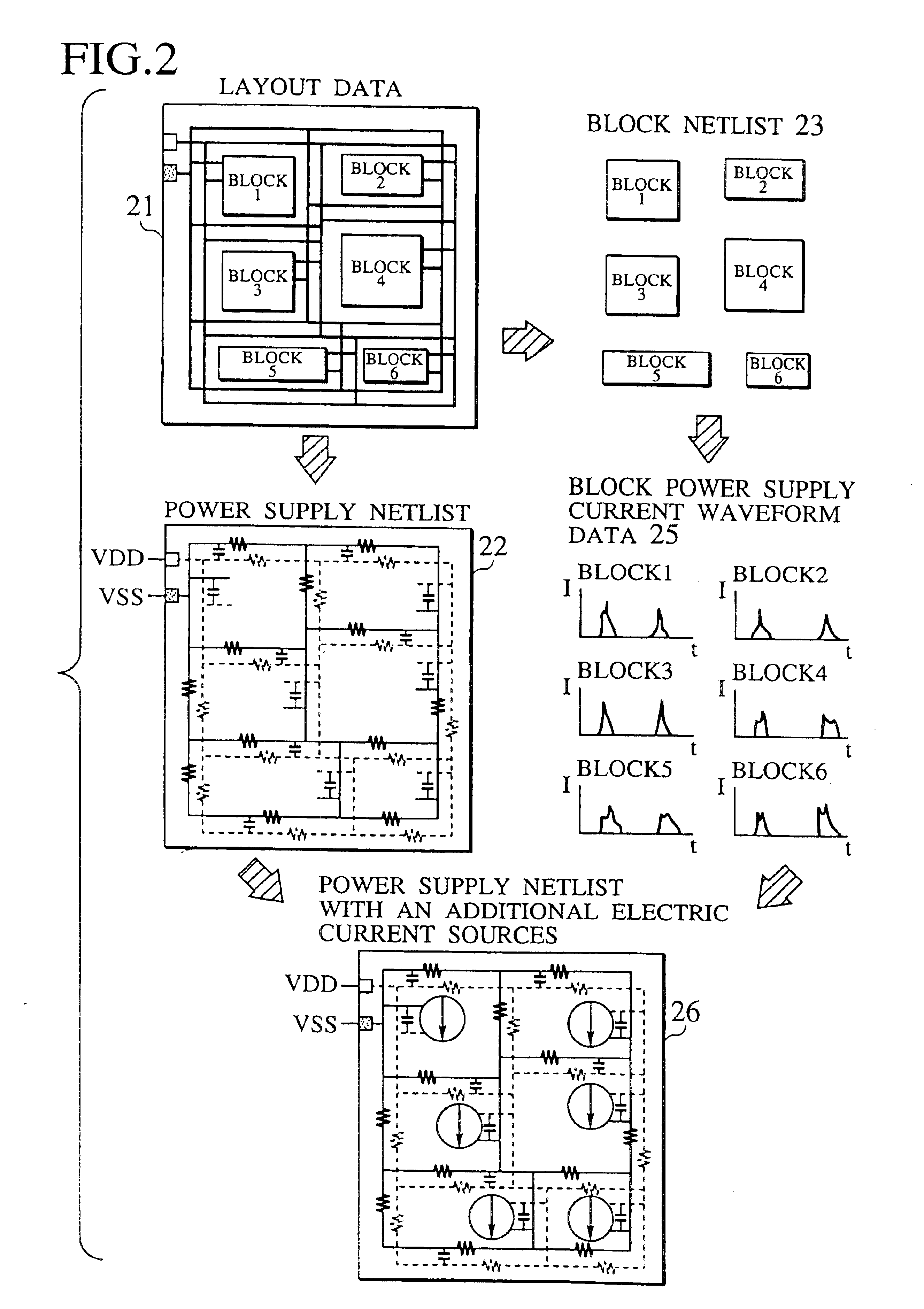
FIG. 1 is a block diagram showing the apparatus for analyzing EMI noise in accordance with the embodiment 1 of the present invention. In FIG. 1 (as well as FIGS. 5, 14 and 16) enclosed in solid lines are functional blocks of the apparatus for analyzing EMI noise. On the other hand, data components and lists are included in broken lines by enclosing with broken lines. FIG. 2 is provided to illustrate the process of preparing a power supply netlist with an additional electric current source(s) by the use of layout data in the noise analyzing apparatus.

The noise analyzing apparatus 10 is composed of a power supply netlist extracting section 11, a block netlist extracting section 12, a block power supply current waveform analyzing section 13, an electric current source adding section 14, a circuit simulating section 15, a Fourier transformation section 16 and a simulation result displaying section 17. Meanwhile, layout data and test vector data as explained in the followin...

embodiment 2

[Embodiment 2]

Generally speaking, in the case of a linear circuit composed only of RLC and powered by a plurality of the electric power sources, the electric current and the voltage level of any one of the constituent elements of the linear circuit are calculated by gumming up the electric current and the voltage level of the same linear circuit which is assumed to be powered only by each of the plurality of the electric power sources in accordance with the so-called principle of superposition. The power supply netlist is a linear circuit composed only of RLC to that the current / voltage data is obtained on the assumption that one of the plurality of the electric power sources in correspondence with each block exists alone. Accordingly, the current / voltage data in the case that an arbitrary number of electric current sources are connected is obtained by summing up the current / voltage data obtained on the assumption that each of the plurality of the electric current sources exists alo...

embodiment 3

[Embodiment 3]

The configuration of the noise analyzing apparatus 30 in accordance with the embodiment 3 is shown in FIG. 16. The noise analyzing apparatus in accordance with the embodiment 3 consists of the noise analyzing apparatus 10 in accordance with the embodiment 1 to which is added a circuit element value modifying section 19. The other constituent elements have the equivalent structures and functions of the counterparts of the previous embodiment as illustrated in FIG. 1 and given the similar references.

The circuit element value modifying section 19 serves to generate the circuit element value modified power supply netlist 33 by modifying the characteristic values of the circuit elements contained in the power supply netlist 26 with an additional electric current source(s) on the basis of circuit element value modification information 32. The circuit element value modification information 32 is the information given in order to modify the characteristic values of the circuit...


PUM


Abstract

A technique for effectively attenuating EMI noise, which is generated from the electric power system of semiconductor devices, is described. In accordance with the technique, a power supply netlist with an additional electric current source(s) is generated by adding block power supply current waveform data, as extracted from test vector data and a block netlist, to the power supply netlist as extracted from the layout data of the circuit under analysis. A circuit simulation of the power supply netlist with an additional electric current source(s) is then performed in order to calculate power supply current/voltage waveform data. Furthermore, current/voltage spectral data is calculated by the Fourier transformation of the power supply current/voltage waveform data followed by displaying the current/voltage spectral data as the result of the Fourier transformation.

Description

BACKGROUND OF THE INVENTION1. Field of the InventionThe present invention is related to a technique for suppressing noise as emitted from semiconductor devices such as integrated circuits, for example, a technique for suppressing EMI noise as emitted from the power supply system of the semiconductor device, noise as originating from the resonance between circuit elements contained in the semiconductor device, and so forth.2. Description of the Related ArtRecently, emission of EMI noise becomes substantially problematic while the packing densities of integrated circuits have been increased. The EMI noise is thought to be generated in accordance with the mechanism as described in the followings. When a number of circuit elements are turned off / on at the same time within an integrated circuit, instantaneous currents are passed through a power source line. This rapidly changing electric current contains a number of high frequency components. Because of this, the wirings formed within th...

Claims


Application Information

Patent Timeline
Patent Type & Authority Patents(United States)
IPC IPC(8): G06F17/50H01L21/66G01R29/08
CPCG06F17/5036G06F30/367
Inventor HAYASHI, SACHIO
Owner KK TOSHIBA
Why Eureka
Try Eureka