Selective refractory metal and nitride capping

a refractory metal and selective technology, applied in the direction of semiconductor devices, semiconductor/solid-state device details, electrical apparatus, etc., can solve the problems of loss of selectivity in some regions, difficult initiation of deposition, and non-uniform film growth, etc., to prevent cu electromigration and diffusion

Inactive Publication Date: 2005-01-18
NOVELLUS SYSTEMS
View PDF4 Cites 224 Cited by
  • Summary
  • Abstract
  • Description
  • Claims
  • Application Information

AI Technical Summary

Benefits of technology

The present invention provides a method for depositing a refractory metal capping layer and creating a refractory metal nitride over this deposited refractory metal effective for preventing Cu electromigration and diffusion in Cu semiconductor devices. The invention involves at least two of the following ope

Problems solved by technology

Using normal bulk deposition procedures, initiation of deposition can be difficult.
As a consequence,

Method used


Image

  • Selective refractory metal and nitride capping
  • Selective refractory metal and nitride capping
  • Selective refractory metal and nitride capping

Examples


Embodiment Construction

Introduction

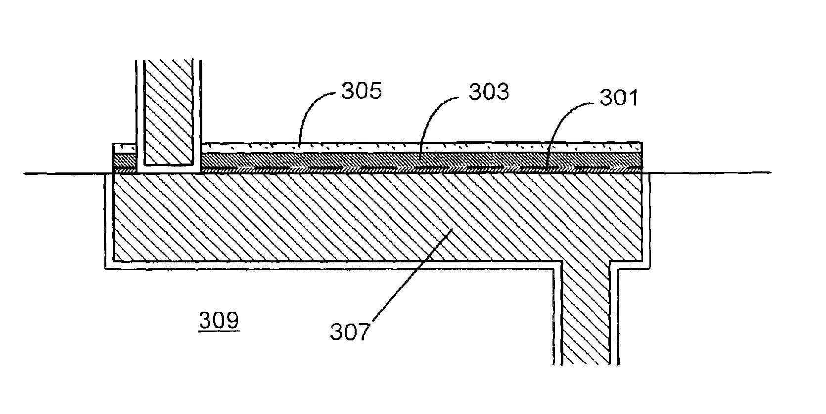
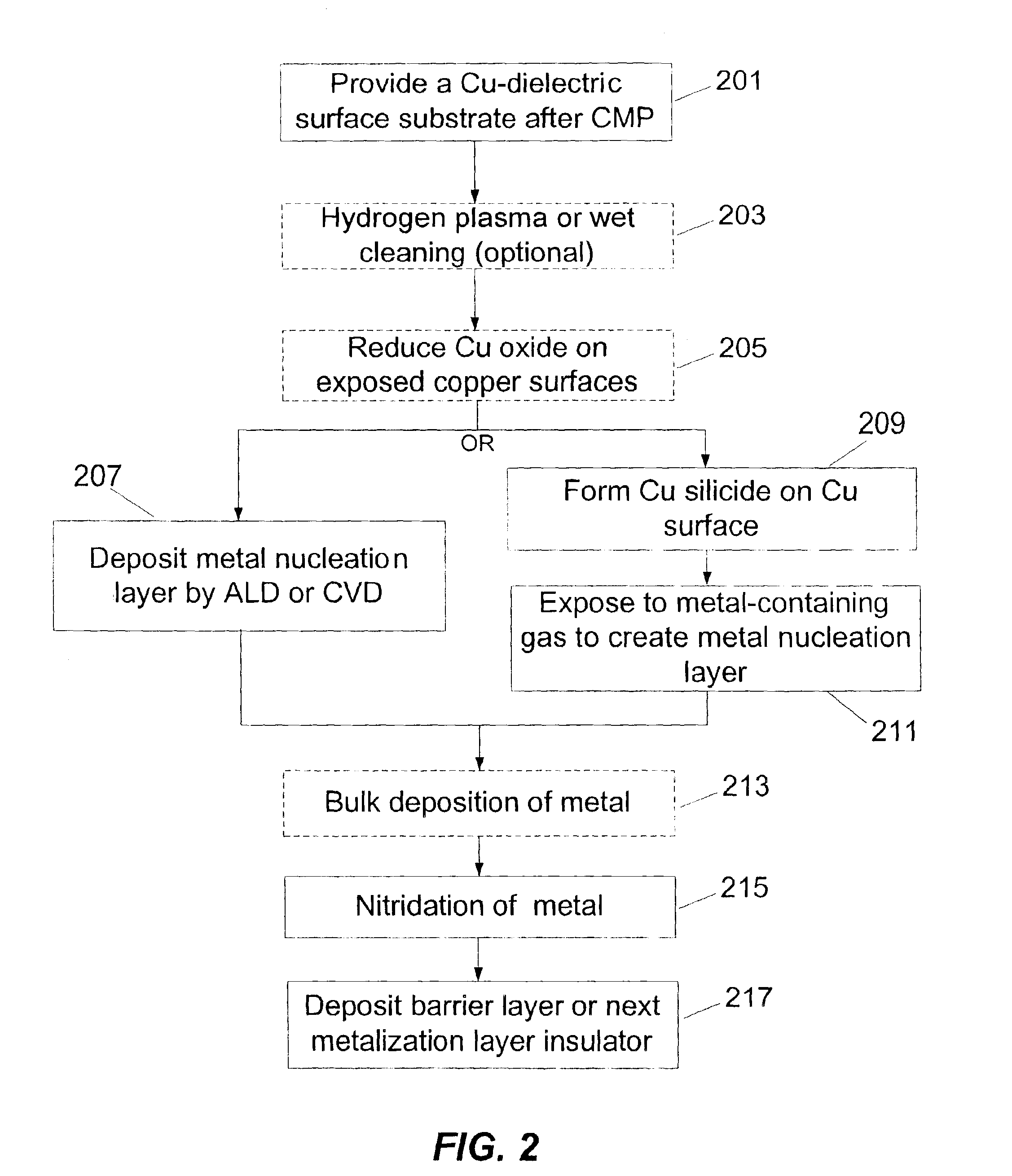
As indicated, the present invention provides a capping layer of a refractory metal. That metal may be formed by first depositing a nucleation layer followed by a bulk layer. In some embodiments, the nucleation layer is all that is required. This may be the case when only a very thin refractory metal layer is required. With or without a bulk layer deposited on the nucleation layer, the invention may also employ a nitride layer formed from some or all of the refractory metal.

A typical process flow for the formation of a capping layer employed in accordance with this invention is illustrated in the flowchart of FIG. 2. First a partially fabricated semiconductor device is provided 201. This device has exposed copper lines in a dielectric support. In the case of a damascene process, the copper lines are inlaid in the dielectric support after the support has had line paths and vias etched therein. Typically the partially fabricated device has a planarized surface comprised of ...


PUM


Abstract

A method for creating a refractory metal and refractory metal nitride cap effective for reducing copper electromigration and copper diffusion is described. The method includes depositing a refractory metal nucleation layer and nitriding at least the upper portion of the refractory metal layer to form a refractory metal nitride. Methods to reduce and clean the copper lines before refractory metal deposition are also described. Methods to form a thicker refractory metal layer using bulk deposition are also described.

Description

FIELD OF THE INVENTIONThis invention pertains to methods for depositing refractory metal and creating a refractory metal nitride over the deposited refractory metal. More specifically, the invention pertains to methods that deposit a layer of refractory metal and refractory metal nitride over copper lines on a semiconductor device so as to prevent electromigration of the copper line and diffusion of copper into substrate material.BACKGROUND OF THE INVENTIONBecause copper has a lower resistivity and higher resistance to electromigration compared to aluminum, it has become the preferred material for creating conductive lines in high performance integrated circuits. Since Cu does not readily form volatile compounds and is therefore difficult to dry etch, the fabrication of Cu interconnects requires a damascene approach, whereby a metal is deposited into a recess etched in an insulating material (dielectric) and then planarized using chemical mechanical polish (CMP). While the damascene...

Claims


Application Information

Patent Timeline
IPC IPC(8): H01L21/02H01L21/4763H01L21/285H01L21/768
CPCH01L21/76849H01L21/76867H01L21/76883H01L21/76856H01L21/28556H01L21/28562H01L21/76889
Inventor FAIR, JAMES A.HAVEMANN, ROBERT H.SUNG, JUNGWANTAYLOR, NERISSALEE, SANG-HYEOBPLANO, MARY ANNE
Owner NOVELLUS SYSTEMS
Why Eureka
Try Eureka