Multi-chip semiconductor package structure

a liquid semiconductor and semiconductor technology, applied in semiconductor devices, semiconductor/solid-state device details, electrical devices, etc., can solve the problems of reducing yield and reliability, increasing overall package volume and packaging cost, and high cost of first lead frame 134/b>, so as to reduce circuit space and reduce production cost

Inactive Publication Date: 2005-01-18
VANGUARD INTERNATIONAL SEMICONDUCTOR CORPORATION
View PDF5 Cites 6 Cited by
  • Summary
  • Abstract
  • Description
  • Claims
  • Application Information

AI Technical Summary

Benefits of technology

Accordingly, one object of the present invention is to provide a multi-chip semiconductor package structure capabl

Problems solved by technology

Under such circumstances, contact between a wire on one chip with a neighboring wire on another chip is highly probable and may lead to short-circuiting.
However, this will increase the overall package volume and packaging cost.
Moreover, using YAG laser to joint the second lead frame 164 onto the first lead frame 134 is an expensive undertaking likely to inc

Method used


Image

  • Multi-chip semiconductor package structure
  • Multi-chip semiconductor package structure
  • Multi-chip semiconductor package structure

Examples


first embodiment

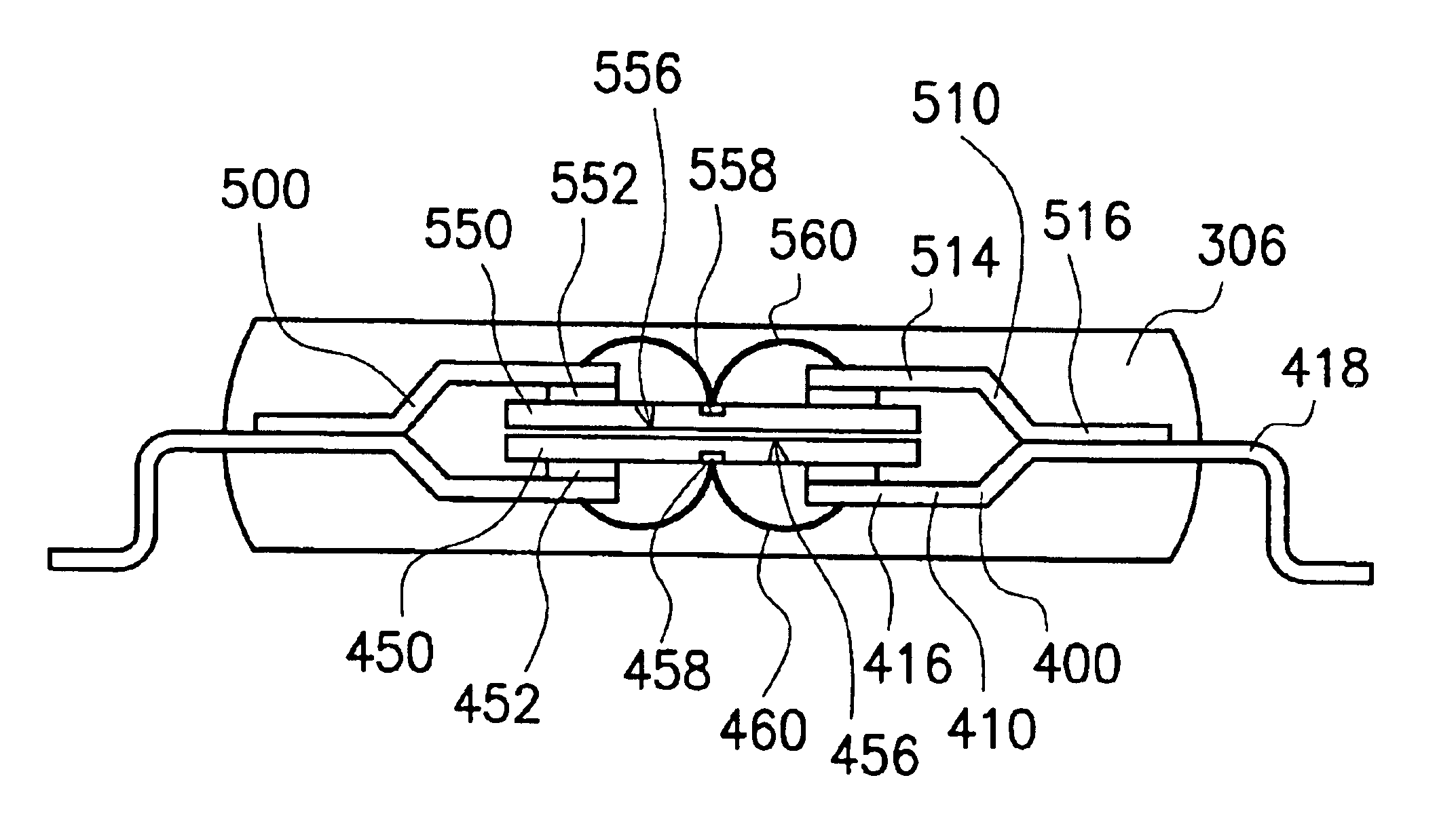
FIG. 7 is a schematic cross-sectional view showing a multi-chip semiconductor package structure according to a second preferred embodiment of this invention. In the first embodiment shown in FIG. 6, the joint sections 516 are located inside the packaging material 306. Hence, the joint sections 516 and the lead frame 400 can have very tight junctions. However, the joint sections 516 are not restricted to the aforementioned position. The joint sections 516 may extend into a region outside the packaging material 306 as shown in FIG. 7. The indentation 520 is now located outside the package body. Therefore, the step of removing the side bar 518 can be conducted before or after package molding.

FIG. 8 is a schematic cross-sectional view showing a multi-chip semiconductor package structure according to a third preferred embodiment of this invention. FIG. 8A is a bottom up view of the lead frame 600 shown in FIG. 8. In the first embodiment, there is a side bar 518 just outside the joint sec...

third embodiment

FIG. 9 is a schematic cross-sectional view showing a multi-chip semiconductor package structure according to a fourth preferred embodiment of this invention. In the third embodiment, the joint sections 606 are exposed outside the packaging material 632. However, the joint sections 606 are not restricted to such a location. The joint sections 606 can be enclosed inside the packaging material 652 as shown in FIG. 9. When the joint sections 606 are inside the package body, dam bar (not shown) and the leads 602 need to be separated before molding.

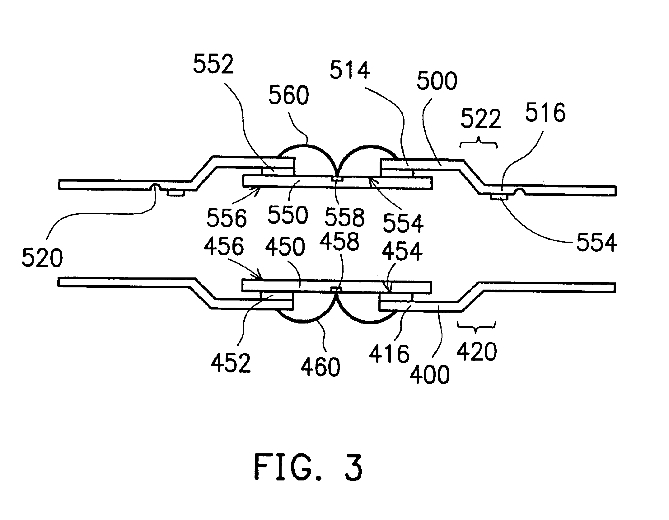
FIG. 10 is a schematic cross-sectional view showing a multi-chip semiconductor package structure according to a fifth preferred embodiment of this invention. FIG. 11 is a schematic cross-sectional view showing a multi-chip semiconductor package structure according to a sixth preferred embodiment of this invention. To prevent conductive wires 460 and 560 from exposing outside the packaging material 306 in the first embodiment (shown in FIG. 6), ...


PUM


Abstract

A multi-chip semiconductor package structure. The structure includes two chips and two lead frames. The leads on one of the lead frames have inner leads at one end and joint sections at the other end. The joint sections are connected with another lead frame. Both lead frames use a common set of external leads. The two chips and two lead frames are joined together forming a lead-on-chip structure with the two chips facing each other back-to-back. The assembly except the external leads is enclosed by packaging material.

Description

BACKGROUND OF THE INVENTION1. Field of InventionThe present invention relates to a multi-chip liquid semiconductor package structure and its method of manufacture. More particularly, the present invention relates to a duplicate chip, duplicate conductive wire package structure capable of shrinking overall package volume while increasing package reliability.2. Description of Related ArtIn this information explosion age, electronic products have enjoyed a close relationship with everybody in this society. Following the rapid progress in electronic technologies, electronic products have become lighter, smaller and more portable. In addition, most electronic products can provide highly personalized functions at an affordable price. Market forces are now pushing semiconductor manufacturers towards manufacturing packages having higher device density to volume ratio. One recent advance of package structure design is the introduction of multi-chip package.FIG. 1 is a schematic cross-section...

Claims


Application Information

Patent Timeline
IPC IPC(8): H01L23/495H01L23/48
CPCH01L23/4951H01L23/49575H01L24/06H01L23/49537H01L24/32H01L2924/01033H01L2224/04042H01L2224/05599H01L2224/06136H01L2224/32014H01L2224/32245H01L2224/48091H01L2224/48247H01L2224/4826H01L2224/49171H01L2224/73215H01L2224/85399H01L2924/01039H01L2924/01082H01L2924/014H01L2924/00014H01L24/49H01L2224/05554H01L24/48H01L2224/45099H01L2924/00H01L2924/00012H01L2924/12042H01L2924/181
Inventor LIAO, KUANG-HOLIN, FENGCHEN, YUN-SHENG
Owner VANGUARD INTERNATIONAL SEMICONDUCTOR CORPORATION
Why Eureka
Try Eureka