Converting bits to vectors in a programmable logic device

a programmable logic and bit vector technology, applied in the direction of computation using denominational number representation, pulse technique, instruments, etc., can solve the problem that components place a significantly larger burden on pld routing resources

Inactive Publication Date: 2005-01-18
LATTICE SEMICON CORP
View PDF14 Cites 7 Cited by
  • Summary
  • Abstract
  • Description
  • Claims
  • Application Information

AI Technical Summary

Benefits of technology

A PLD is disclosed that uses vector components (e.g., vector processing blocks) as a dedicated PLD resource. Vector components require input information to be provided in vectors (e.g., 8 bits, 16 bits, 32 bits, 64 bits, etc.). However, logic blocks in the PLD traditionally manipulate information as unordered bits. Thus, routing between PLD logic blocks to vector components places a significantly larger burden on PLD routing resources than would otherwise be required to route information between PLD logic blocks. Consequently, an interface is disclosed that converts unordered bits in a PLD domain to vectors in a vector domain. The interface may also perform formatting functions, such as scaling and / or sign extension, on the unordered bits to further free up expensive resources in the PLD domain.

Problems solved by technology

However, logic blocks in the PLD traditionally manipulate information as unordered bits.
Thus, routing between PLD logic blocks to vector components places a significantly larger burden on PLD routing resources than would otherwise be required to route information between PLD logic blocks.

Method used


Image

  • Converting bits to vectors in a programmable logic device
  • Converting bits to vectors in a programmable logic device
  • Converting bits to vectors in a programmable logic device

Examples


Embodiment Construction

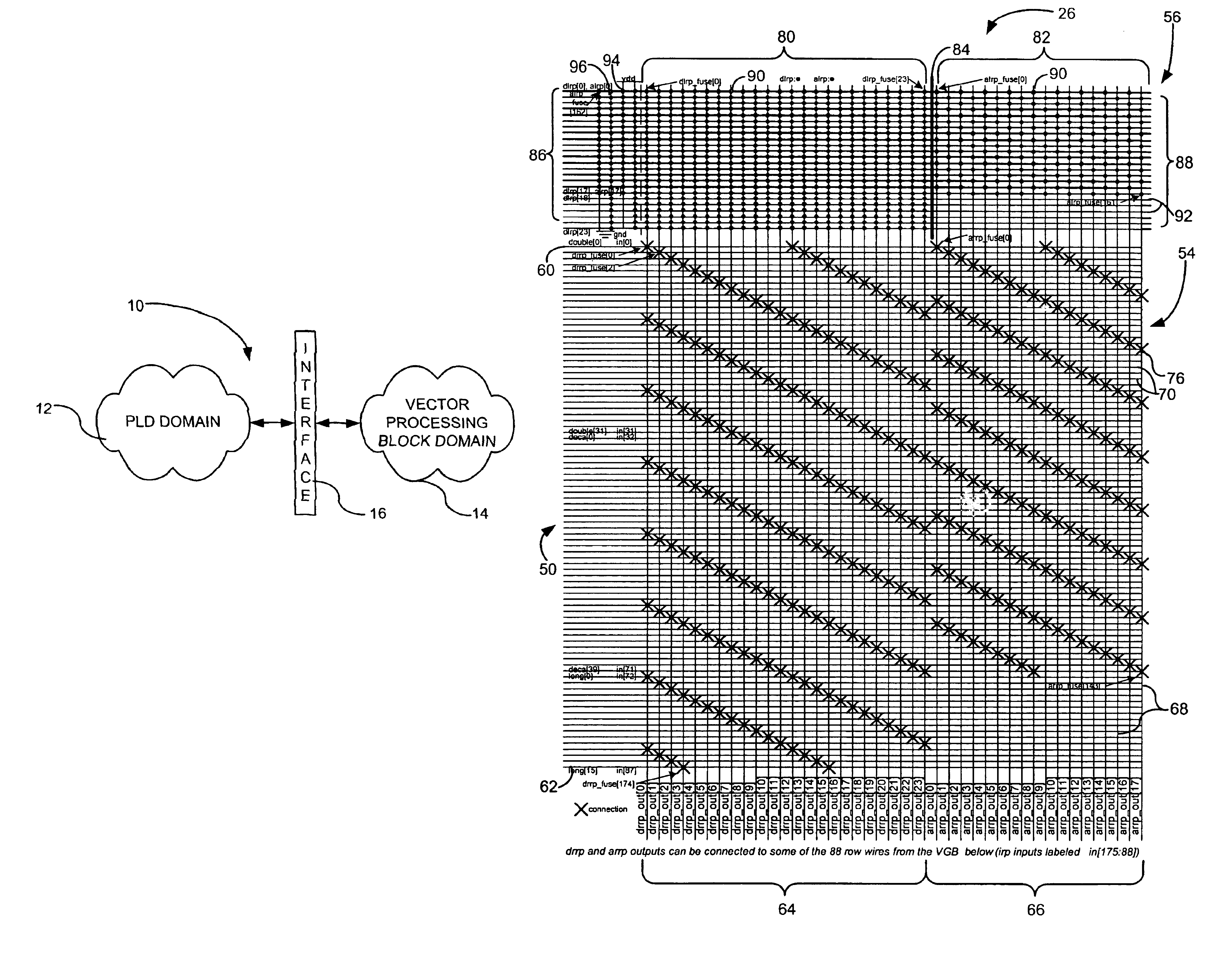
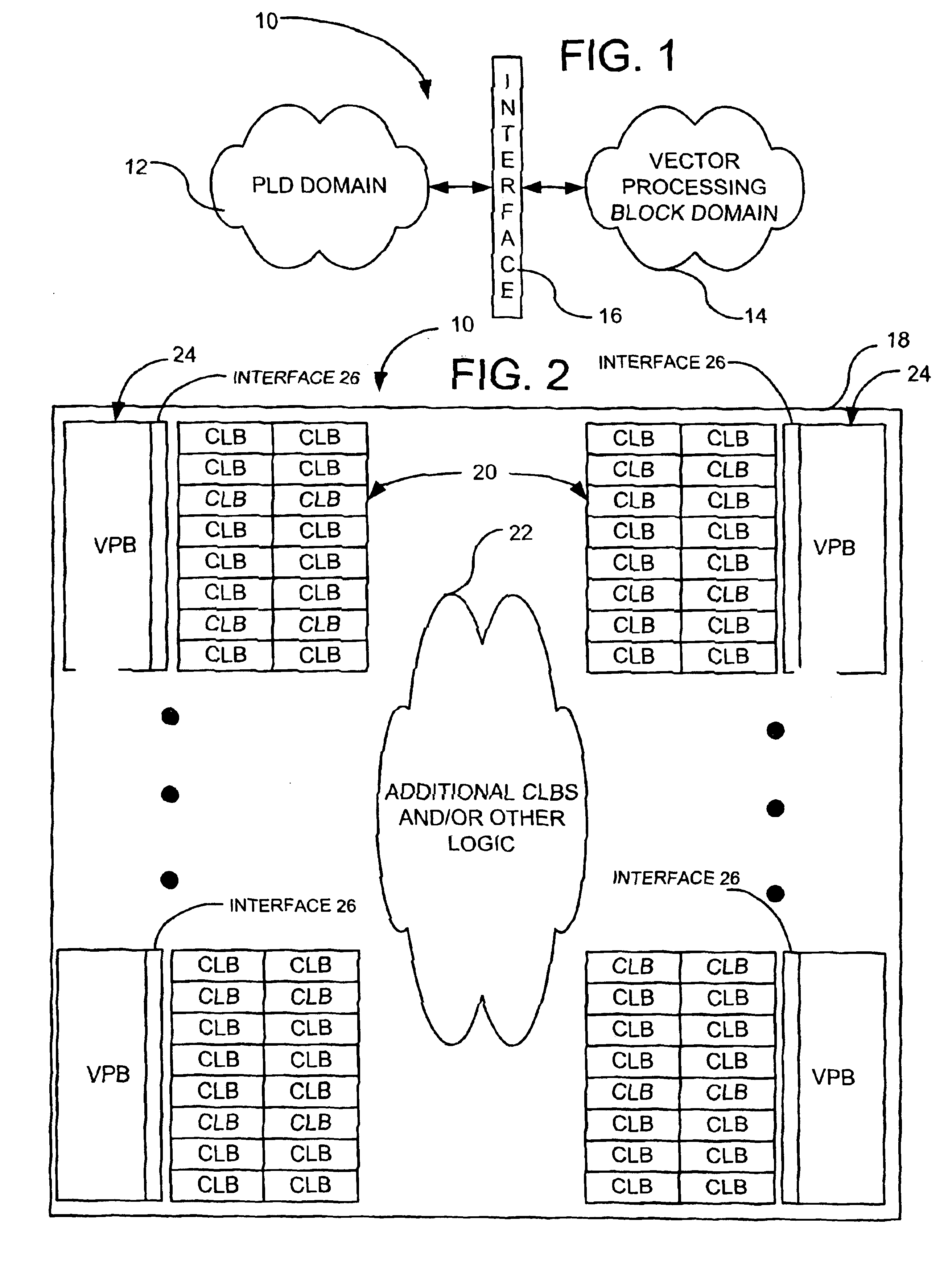
FIG. 1 shows a high-level diagram of a PLD 10 in accordance with the invention including a PLD domain 12, a vector domain 14, and an interface 16 between the two domains 12 and 14. The PLD may be one of many types of programmable devices, such as a field programmable gate array (FPGA). The PLD domain may include conventional fine-grain logic, memory and routing resources where signals are switched and routed on a bit-by-bit basis. Such bit-by-bit manipulation is termed unordered because the bits are not arranged in a predetermined order throughout the domain. The vector domain 14 may include course-grain logic blocks (also referred to herein as vector processing blocks, or VPBs) that perform functions on digital words (integer operands) that include multiple bits grouped together (e.g., 16, 32, 64 bits, etc) in a predetermined order throughout the domain. These words of ordered bits are referred to as vectors. In the vector domain 14, groups of wires are routed together as a vector ...


PUM


Abstract

A circuit is disclosed for a programmable logic device (PLD) environment that converts unordered bits in a PLD domain to fixed-width vectors in a vector domain. The fixed-width vectors may be used within a vector processing block (VPB) that operates on data in vector format. The PLD includes multiple programmable logic blocks that are configurable by a user. The logic blocks operate on data at a bit level resulting in unordered bits of information in a PLD domain. However, a vector processing block operates on data on a vector level (e.g., 8 bits, 16 bits, 32 bits, 64 bits, etc.). Thus, an interface is coupled between the programmable logic blocks and the vector processing block that converts at least a portion of the unordered bits of information from the PLD domain to one or more fixed-width vectors for use in the vector processing block. The interface may also perform scaling and / or sign extension on the unordered bits, to further free up expensive resources in the PLD domain.

Description

TECHNICAL FIELDThe present invention relates to programmable logic devices (PLDs) such as field programmable gate arrays (FPGAs) and CPLDs. More particularly, the present invention relates to an interface for ordering and formatting data bits within a PLD.BACKGROUNDNon-volatile memory devices, such as EPROM, EEPROM, and Flash EEPROM, store data even after power is turned off. One common application of EEPROMs is in programmable logic devices (PLDs). PLDs are standard semiconductor components purchased by systems manufacturers in a “blank” state that can be custom configured or programmed (the terms are used interchangeably in the art) into a virtually unlimited number of specific logic functions. PLDs provide system designers with the ability to quickly create custom logic functions to provide product differentiation without sacrificing rapid time to market. PLDs may be reprogrammable, meaning that the logic configuration can be reconfigured after the initial programming.A type of P...

Claims


Application Information

Patent Timeline
Patent Type & Authority Patents(United States)
IPC IPC(8): H03K19/177
CPCH03K19/17732G06F7/49936G06F7/49994
Inventor DANTE, CONRAD
Owner LATTICE SEMICON CORP
Why Eureka
Try Eureka