Exposure device and method for compensating optical defects

a technology of optical defects and exposure devices, applied in the field of exposure devices and methods for compensating optical defects, can solve problems such as deviations from electronic artwork patterns

Inactive Publication Date: 2005-01-18
XEIKON PREPRESS NV
View PDF7 Cites 23 Cited by
  • Summary
  • Abstract
  • Description
  • Claims
  • Application Information

AI Technical Summary

Benefits of technology

In one embodiment of the invention, during the exposure process, a locus-dependent intensity modulation of the stored artwork pattern can be provided with an electronically stored gray mask. The gray mask is comprised of a set of multiplication factors for each individual image point. During the exposure, the intensity of each individual image point that the light modulator allows to pass through is increased or de...

Problems solved by technology

Due to optical defects and tolerances in the beam path of the exposure device, the projection exposed ...

Method used


Image

  • Exposure device and method for compensating optical defects
  • Exposure device and method for compensating optical defects

Examples


Embodiment Construction

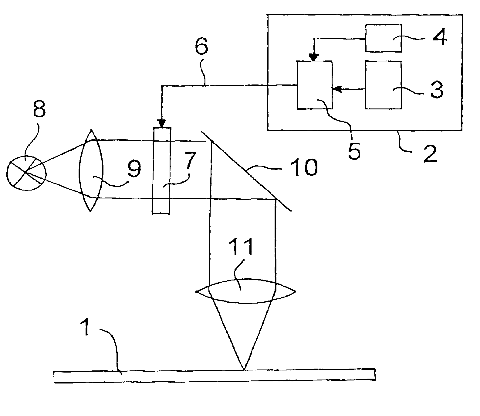
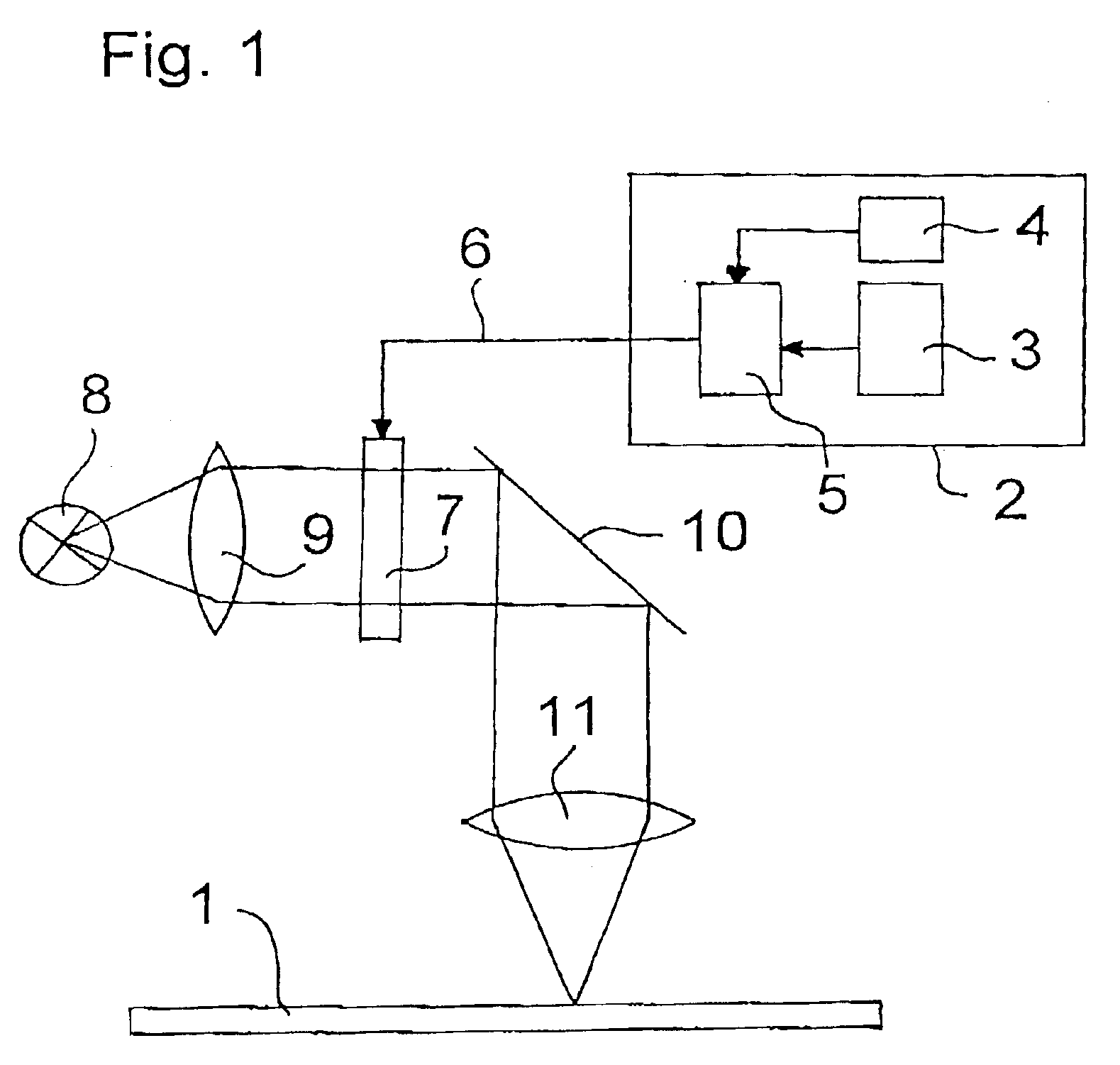
The artwork pattern to be projected onto a printing plate 1 is stored in an image memory 3 in a computer that serves as the processing electronics 2. An overlay file is stored in the overlay memory 4 and is used to generate an electronic gray mask. An image from the image memory 3 or a partial image of the overall image is loaded into a compensator 5 and is corrected pixel by pixel with the overlay data from the overlay memory 4, i.e. the control data provided for controlling the light intensity and / or the duration of the exposure of each individual pixel are modified through multiplication with the correction values of the overlay file in accordance with the desired correction. As a rule, their value is increased or decreased. Then, the corrected image or partial image travels via the data line 6 to the light modulator, in this case an LCD display through which radiation passes, in whose focal plane the actual image is produced.

An illumination device for illuminating the light modu...


PUM


Abstract

An exposure device for exposing a projection of an electronically stored artwork pattern onto a substrate, in particular a printing plate 1, with image processing electronics (2) that can store the image data, with a light modulator (7) that can be electronically controlled by the image processing electronics (2), in particular an LCD display (7) or a micro-mirror device, with an illuminating device (8, 9) for illuminating the light modulator (7), and with a projection lens (11) for projecting the light modulator (7) onto the substrate (1), is improved according to the invention in that the image processing electronics (2) include a compensation device (4, 5) to compensate for optical defects and/or tolerances in the beam path of the exposure device.

Description

BACKGROUND OF THE INVENTIONThe invention relates to an exposure device for exposing a projection of an electronically stored artwork pattern onto a substrate, in particular a printing plate, with image processing electronics that can store the image data, with a light modulator that can be electronically controlled by the image processing electronics, in particular an LCD display or a micro-mirror device, with an illuminating device for illuminating the light modulator and with a projection lens for projecting the light modulator onto the substrate. The invention also relates to a method for compensating for optical defects and / or tolerances in the beam path of such an exposure device.An exposure device of this kind, which is used to expose printing plates with ultraviolet light, is known from DE 195 45 821 A1, for example. In this instance, the artwork pattern to be projected is broken down into partial images by a computer and the partial images are cast one after the other onto a...

Claims


Application Information

Patent Timeline
IPC IPC(8): G03F7/20G03B27/32G02B26/08
CPCG03F7/70433G03F7/70291
Inventor LUELLAU, FRIEDRICH
Owner XEIKON PREPRESS NV
Why Eureka
Try Eureka