Non-volatile latch circuit and a driving method thereof

a latch circuit and non-volatile technology, applied in the direction of pulse generators, pulse techniques, instruments, etc., can solve the problems of ferroelectric film properties deteriorating, power consumption also increasing, and power consumption increasing serious problems

Active Publication Date: 2005-01-18
PANASONIC CORP
View PDF8 Cites 56 Cited by
  • Summary
  • Abstract
  • Description
  • Claims
  • Application Information

AI Technical Summary

Benefits of technology

[0017]the voltage that is generated at the second electrode by residual polarization in the ferroelectric film being higher than the threshold voltage of the inverter element when the voltage is applied to the first input terminal and the switching element is turned off.

Problems solved by technology

However, since leakage current increases when an MIS transistor, etc., is miniaturized, power consumption also increases.
In particular, in DRAMs, SRAMs, etc., that use MIS transistors in their memory cells, an increase of power consumption poses a serious problem.
Accordingly, the properties of the ferroelectric film deteriorate due to the increased number of voltage applications required to read data.

Method used


Image

  • Non-volatile latch circuit and a driving method thereof
  • Non-volatile latch circuit and a driving method thereof
  • Non-volatile latch circuit and a driving method thereof

Examples


first embodiment

[0046

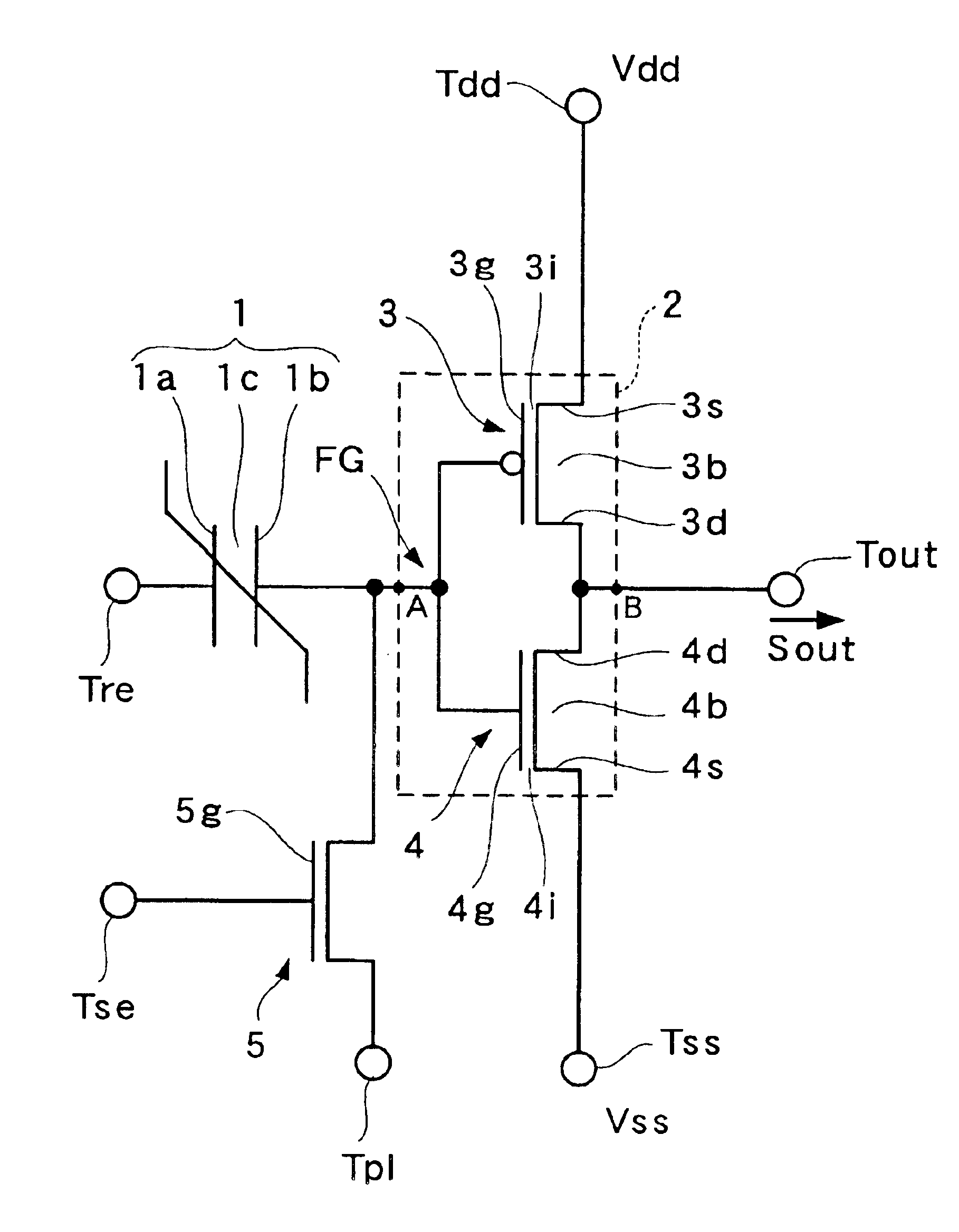
[0047]Hereunder, the first embodiment of the non-volatile latch circuit will be explained with reference to the drawings. FIG. 1 is a diagram schematically showing the structure of a non-volatile latch circuit of the present embodiment.

[0048]As shown in FIG. 1, non-volatile latch circuit 10 is provided with ferroelectric capacitor 1, CMOS inverter element 2, which comprises PMISFET 3 and NMISFET 4, and reset NMISFET 5.

[0049]Ferroelectric capacitor 1 is formed of first and second electrodes 1a and 1b, and ferroelectric film 1c inserted between first and second electrodes 1a and 1b. First electrode 1a is connected to reset terminal Tre (first input terminal), and second electrode 1b is connected to gate electrode 3g of PMISFET 3 and gate electrode 4g of NMISFET 4 through conductive members, such as a plug and electric wiring. There are many examples of ferroelectric materials that can form ferroelectric film 1c, for example, strontium bismuth tantalate (Y1: SrBi2TaO9). When the c...

second embodiment

[0126

[0127]FIG. 7 is a block diagram showing the structure of the semiconductor integrated circuit of the second embodiment of the invention.

[0128]As shown in this diagram, the semiconductor integrated circuit of the present embodiment comprises two logic blocks 11 and 12. These integrate a great many logic transistors, etc. Logic blocks 11 and 12 are connected to each other by wiring 13 via pass-transistor 14 (NMISFET). Non-volatile latch circuit 10 described in the first embodiment is connected to pass-transistor 14. Output signal Sout of non-volatile latch circuit 10 is applied to the gate of pass-transistor 14 in such a manner that the on- or off-state of pass-transistor 14 can be controlled.

[0129]Because the on- or off-state of pass-transistor 14 that is disposed between logic blocks 11 and 12 is controlled by output signal Sout of non-volatile latch circuit 10 in the above-described structure, when power supply is restored after power supply to the entire semiconductor integra...

third embodiment

[0137

[0138]FIG. 9 is a block diagram showing the structure of the semiconductor integrated circuit of the third embodiment of the invention. As shown in this figure, the semiconductor integrated circuit of this embodiment is a 4-input multiplexer circuit, which comprises four input terminals Tin 1-Tin 4 and one output terminal Tout′, the circuit being designed so that one of input signals from input terminals Tin 1-Tin 4 is selected by two-step select circuits 30A and 30B and output from output terminal Tout′. First select circuit 30A comprises non-volatile latch circuit 10A of the first embodiment, four pass-transistors 20A-20D that receive input signals from input terminals Tin 1-Tin 4, respectively, and inverter 21 that inverts output from non-volatile latch circuit 10A.

[0139]The gate of pass-transistor 20A, which is one of two pass-transistors 20A and 20B that receive input from input terminals Tin 1 and Tin 2, receives output signal Sout 1 from non-volatile latch circuit 10A. T...


PUM


Abstract

Non-volatile latch circuit 10 of the present invention comprises ferroelectric capacitor 1 provided with a first electrode 1a, second electrode 1b, and ferroelectric film 1c that lies between these electrodes; reset terminal Tre that is connected to first electrode 1a and a CMOS inverter element 2 that is connected to second electrode 1b of ferroelectric capacitor 1; voltage switching terminal Tpl that applies a voltage to second electrode 1b; switching element 5 that is connected between second electrode 1b and second input terminal Tpl and switches a voltage applied to second electrode 1b; and set terminal Tse that applies a voltage for switching on or off switching element 5, wherein the voltage generated in second electrode 1b caused by polarization retained by ferroelectric film 1c is higher than the threshold voltage Vtn of NMISFET 4 of CMOS inverter element 2.

Description

[0002]This application is a continuation of PCT / JP03 / 15958, filed Dec. 12, 2003.TECHNICAL FIELD[0003]This invention relates to a latch circuit that has a non-volatile memory function using a ferroelectric material, and a driving method thereof.BACKGROUND ART[0004]In recent years, the integration of semiconductor integrated circuits has made significant advances due to the miniaturization of constituent MIS transistors. However, since leakage current increases when an MIS transistor, etc., is miniaturized, power consumption also increases. In particular, in DRAMs, SRAMs, etc., that use MIS transistors in their memory cells, an increase of power consumption poses a serious problem.[0005]For this reason, in recent years, non-volatile memories, which retain information even when power is removed, attracted considerable attention. Because of the above-described property, a non-volatile memory does not require any operation to restore the condition that it was in at the time that the powe...

Claims


Application Information

Patent Timeline
Patent Type & Authority Patents(United States)
IPC IPC(8): H03K17/693G11C11/22H01L21/8246H01L27/105H03K3/356H03K19/0948H03K19/185
CPCG11C11/22H03K17/693
Inventor TOYODA, KENJIOHTSUKA, TAKASHIMORIMOTO, KIYOSHI
Owner PANASONIC CORP
Why Eureka
Try Eureka