MEMS direct chip attach packaging methodologies and apparatuses for harsh environments

a technology of direct chip and packaging method, applied in the direction of fluid pressure measurement, microstructured devices, instruments, etc., can solve the problems of increasing the risk of sealing agent sipping into the reference cavity, rendering the device useless, and conventional semiconductor electronic and sensing devices limited to operating in temperatures

Inactive Publication Date: 2005-01-25
NAT AERONAUTICS & SPACE ADMINISTATION UNITED STATES OF AMERICA AS REPRESENTED BY THE ADMINSTRATOR OF THE
View PDF29 Cites 84 Cited by
  • Summary
  • Abstract
  • Description
  • Claims
  • Application Information

AI Technical Summary

Benefits of technology

The basic components comprise a bottom substrate member of a dielectric material with thermomechanical properties similar or closely similar to that of silicon carbide, silicon or aluminum nitride. The bottom cover substrate member serves as a receiving platform for the silicon carbide sensors. The sensors may also be made of aluminum nitride or silicon. It also serves as the first level of protection of the sensor from harmful particulates in the high temperature environments in which the sensor is employed. Typically, the bottom substrate has a hole or aperture therein which allows pressure and / or temperature to be transmitted to the sensor. The top cover substrate made from the same material as the bottom substrate provide sandwiched protection for the sensors. Because they are made of the same material with thermomechanical properties similar to that of the sensors, the problem of mismatch in the coefficient of thermal expansion associated with the prior art is significantly reduced.

Problems solved by technology

This may lead to debonding during thermal cycling thereby rendering the device useless.
Since the aperture will have to be sealed later in order to maintain the desired hermetic reference cavity, it increases the risk of the sealant sipping into the reference cavity.
Package reliability problems have largely contributed to prevent the application of these devices.
This is very challenging since conventional semiconductor electronic and sensing devices are limited to operating in temperatures less than 300° C. due to the limitations imposed by material properties and packaging.
However, the lack of the device (sensor) packaging methodologies appropriate for this harsh environment has affected the operational reliability and survivability of these devices (sensors).
Reliability problems at high temperature due to poor packaging has discouraged global application and large-scale commercialization of these devices.
As such, the much anticipated introduction of SiC devices into high temperature environments has been delayed.

Method used


Image

  • MEMS direct chip attach packaging methodologies and apparatuses for harsh environments
  • MEMS direct chip attach packaging methodologies and apparatuses for harsh environments
  • MEMS direct chip attach packaging methodologies and apparatuses for harsh environments

Examples


Embodiment Construction

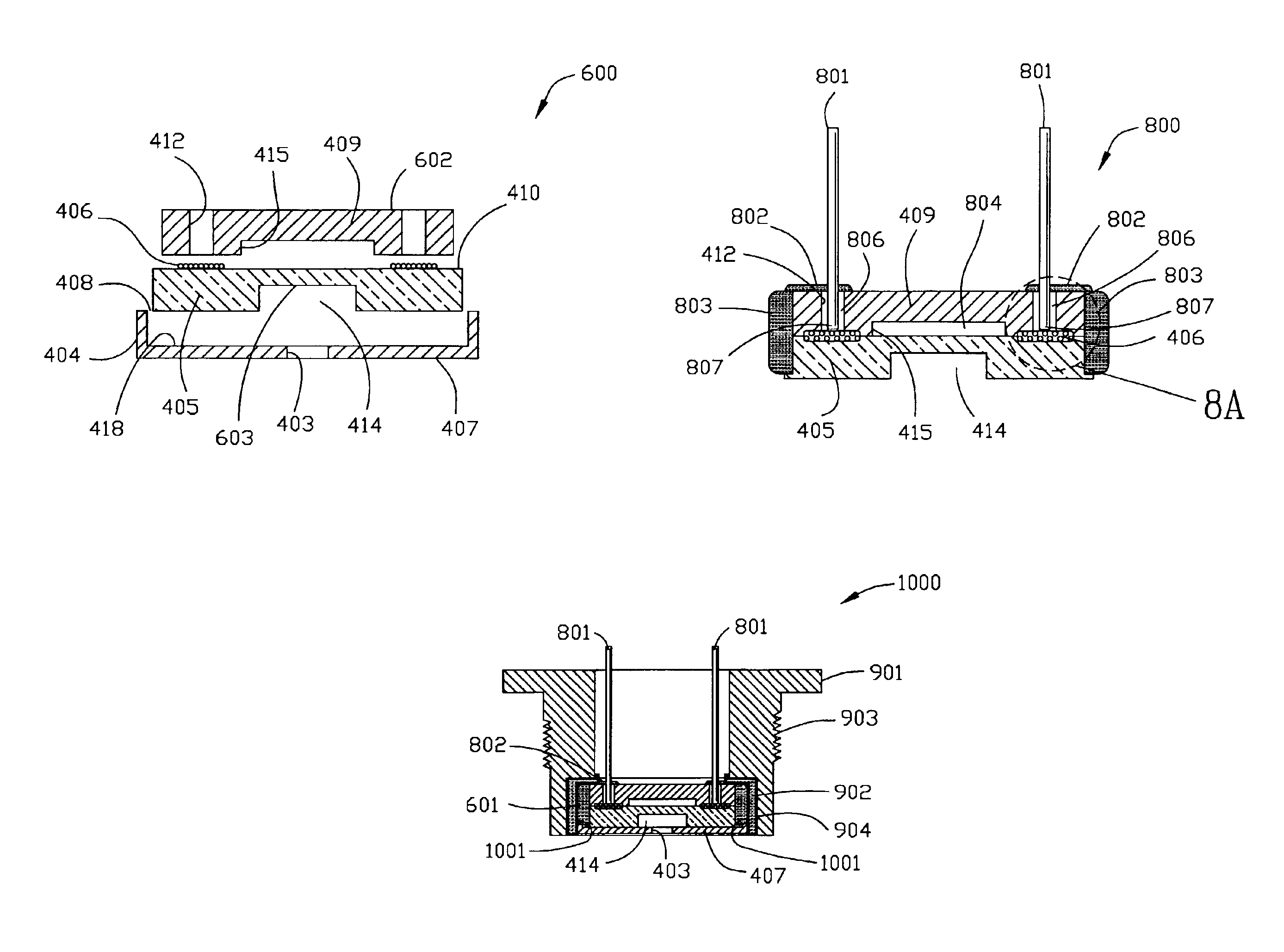
FIG. 4 is a plan view 400 of the instant invention illustrating a section of the array of the bottom cover or substrate 402, a sensor 405 in the housing of one cell 407 of the bottom cover substrate 400, and a sensor 405 in another cell 407 of the bottom cover substrate along with the top cover 409 residing above the sensor 405. Top cover 409 is illustrated diagrammatically and is shown not connected to the array of which it is a part.

In one embodiment, each sensor or electronics chip 405 is dropped into the corresponding cells 407 arranged in an array 400 as shown in FIG. 4. The cell-array 400 is made from material that will survive high temperatures up to 700° C. such as aluminum nitride or silicon carbide, preferably in amorphous form for reduced cost without loss of performance. It will also have thermomechanical properties close to that of the material in which the chip 405 is made. Typically, the sensor chip will be made from silicon carbide or aluminum nitride as taught in my...


PUM


Abstract

Methods of bulk manufacturing high temperature sensor sub-assembly packages are disclosed and claimed. Sensors are sandwiched between a top cover and a bottom cover so as to enable the peripheries of the top covers, sensors and bottom covers to be sealed and bound securely together are disclosed and claimed. Sensors are placed on the bottom covers leaving the periphery of the bottom cover exposed. Likewise, top covers are placed on the sensors leaving the periphery of the sensor exposed. Individual sensor sub-assemblies are inserted into final packaging elements which are also disclosed and claimed. Methods of directly attaching wires or pins to contact pads on the sensors are disclosed and claimed. Sensors, such as pressure sensors and accelerometers, and headers made out of silicon carbide and aluminum nitride are disclosed and claimed. Reference cavities are formed in some embodiments disclosed and claimed herein where top covers are not employed.

Description

FIELD OF THE INVENTIONThe innovation describes various methods of fabricating packages used for protection of electronics and sensors in high temperature environments. Apparatuses made by the various methods of fabricating sensor sub-assemblies and their final packaging are also disclosed.BACKGROUND OF THE INVENTIONMy copending U.S. patent application Ser. No. 10 / 124,689; filed Apr. 12, 2002, entitled MULTI-FUNCTIONAL MICRO ELECTROMECHANICAL DEVICES AND METHOD OF BULK MANUFACTURING SAME discloses and claims a method of bulk manufacturing SiC sensors, including pressure sensors and accelerometers. The disclosure of my copending application is incorporated herein by reference.I am a named inventor of U.S. Pat. No. 5,637,905 to Carr et al. and it discloses a high temperature pressure and displacement microsensor made from a Si substrate. A first coil structure is positioned within a recess in the Si substrate. A pressure diaphragm is glass bonded about its periphery to the rim of the r...

Claims


Application Information

Patent Timeline
Patent Type & Authority Patents(United States)
IPC IPC(8): G01D11/24
CPCB81B7/0061G01D11/245B81C1/00301B81B2201/0264B81B2207/095
Inventor OKOJIE, ROBERT S.
Owner NAT AERONAUTICS & SPACE ADMINISTATION UNITED STATES OF AMERICA AS REPRESENTED BY THE ADMINSTRATOR OF THE
Why Eureka
Try Eureka